PIC12F609/615/12HV609/615
3.3.4
EXTERNAL RC MODES
3.4
Internal Clock Modes
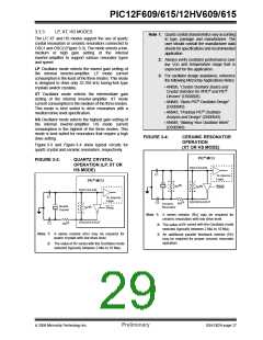
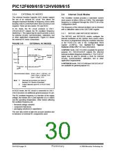
The external Resistor-Capacitor (RC) modes support
the use of an external RC circuit. This allows the
designer maximum flexibility in frequency choice while
keeping costs to a minimum when clock accuracy is not
required. There are two modes: RC and RCIO.
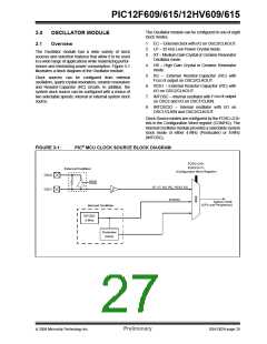
The Oscillator module provides a selectable system
clock source of either 4 MHz or 8 MHz. The selectable
frequency is configured through the IOSCFS bit of the
Configuration Word.
The frequency of the internal oscillator can be trimmed
with a calibration value in the OSCTUNE register.
In RC mode, the RC circuit connects to OSC1.
OSC2/CLKOUT outputs the RC oscillator frequency
divided by 4. This signal may be used to provide a clock
for external circuitry, synchronization, calibration, test
or other application requirements. Figure 3-5 shows
the external RC mode connections.
3.4.1 INTOSC AND INTOSCIO MODES
The INTOSC and INTOSCIO modes configure the
internal oscillators as the system clock source when
the device is programmed using the oscillator selection
or the FOSC<2:0> bits in the Configuration Word
register (CONFIG). See Section 11.0 “Special
Features of the CPU” for more information.
FIGURE 3-5:
EXTERNAL RC MODES
VDD
PIC® MCU
In INTOSC mode, OSC1/CLKIN is available for general
purpose I/O. OSC2/CLKOUT outputs the selected
internal oscillator frequency divided by 4. The CLKOUT
signal may be used to provide a clock for external
circuitry, synchronization, calibration, test or other
application requirements.
REXT
OSC1/CLKIN
Internal
Clock
CEXT
VSS
In INTOSCIO mode, OSC1/CLKIN and OSC2/CLKOUT
are available for general purpose I/O.
(1)
FOSC/4 or
I/O
OSC2/CLKOUT
(2)
Recommended values: 10 kΩ ≤ REXT ≤ 100 kΩ, <3V
3 kΩ ≤ REXT ≤ 100 kΩ, 3-5V
CEXT > 20 pF, 2-5V
Note 1: Alternate pin functions are listed in
Section 1.0 “Device Overview”.
2: Output depends upon RC or RCIO Clock
mode.
In RCIO mode, the RC circuit is connected to OSC1.
OSC2 becomes an additional general purpose I/O pin.
The RC oscillator frequency is a function of the supply
voltage, the resistor (REXT) and capacitor (CEXT) values
and the operating temperature. Other factors affecting
the oscillator frequency are:
• threshold voltage variation
• component tolerances
• packaging variations in capacitance
The user also needs to take into account variation due
to tolerance of external RC components used.
DS41302A-page 28
Preliminary
© 2006 Microchip Technology Inc.

 MICROCHIP [ MICROCHIP ]