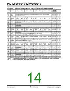
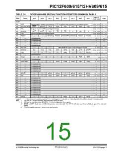
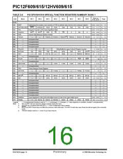
PIC12F609/615/12HV609/615
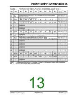
TABLE 2-2:
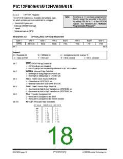
PIC12F615/HV615 SPECIAL FUNCTION REGISTERS SUMMARY BANK 0
Value on
POR, BOR
Addr
Name
Bit 7
Bit 6
Bit 5
Bit 4
Bit 3
Bit 2
Bit 1
Bit 0
Page
Bank 0
00h
01h
02h
03h
04h
05h
06h
07h
08h
09h
0Ah
0Bh
0Ch
0Dh
0Eh
0Fh
10h
11h
INDF
Addressing this location uses contents of FSR to address data memory (not a physical register)
Timer0 Module’s Register
xxxx xxxx 22, 101
xxxx xxxx 41, 101
0000 0000 22, 101
0001 1xxx 15, 101
xxxx xxxx 22, 101
--x0 x000 31, 101
TMR0
PCL
Program Counter’s (PC) Least Significant Byte
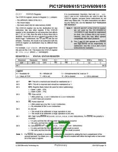
STATUS
FSR
IRP(1)
RP1(1)
RP0
TO
PD
Z
DC
C
Indirect Data Memory Address Pointer
GPIO
—
—
GP5
GP4
GP3
GP2
GP1
GP0
—
Unimplemented
Unimplemented
Unimplemented
Unimplemented
—
—
—
—
—
—
—
—
—
—
—
—
PCLATH
INTCON
PIR1
—
—
Write Buffer for upper 5 bits of Program Counter
---0 0000 22, 101
0000 0000 17, 101
GIE
PEIE
ADIF
T0IE
INTE
—
GPIE
CMIF
T0IF
—
INTF
GPIF
—
CCP1IF
TMR2IF
TMR1IF -00- 0-00 19, 101
—
Unimplemented
—
—
TMR1L
TMR1H
T1CON
TMR2
T2CON
CCPR1L
CCPR1H
CCP1CON
PWM1CON
ECCPAS
—
Holding Register for the Least Significant Byte of the 16-bit TMR1 Register
Holding Register for the Most Significant Byte of the 16-bit TMR1 Register
xxxx xxxx 45, 101
xxxx xxxx 45, 101
T1GINV
TMR1GE T1CKPS1 T1CKPS0 T1OSCEN T1SYNC
TMR1CS
TMR1ON 0000 0000 49, 101
0000 0000 51, 101
Timer2 Module Register
12h
13h
14h
15h
16h
17h
18h
19h
1Ah
1Bh
1Ch
1Dh
1Eh
1Fh
—
TOUTPS3 TOUTPS2 TOUTPS1 TOUTPS0 TMR2ON T2CKPS1 T2CKPS0 -000 0000 52, 101
Capture/Compare/PWM Register 1 Low Byte
Capture/Compare/PWM Register 1 High Byte
XXXX XXXX 76, 101
XXXX XXXX 76, 101
P1M
—
DC1B1
PDC5
DC1B0
PDC4
CCP1M3
PDC3
CCP1M2
PDC2
CCP1M1
PDC1
CCP1M0 0-00 0000 75, 101
PRSEN
PDC6
PDC0
0000 0000 91, 101
ECCPASE ECCPAS2 ECCPAS1 ECCPAS0 PSSAC1
Unimplemented
PSSAC0
PSSBD1
PSSBD0 0000 0000 88, 101
—
—
VRCON
CMCON0
—
CMVREN
CMON
—
VRR
FVREN
CMPOL
VR3
—
VR2
VR1
—
VR0
0-00 0000 62, 101
0000 -0-0 58, 101
COUT
CMOE
CMR
CMCH
—
—
—
—
CMCON1
—
—
—
—
T1ACS
CMHYS
—
T1GSS
CMSYNC ---0 0-10 59, 101
Unimplemented
—
—
ADRESH
ADCON0
Most Significant 8 bits of the left shifted A/D result or 2 bits of right shifted result
ADFM VCFG CHS2 CHS1 CHS0 GO/DONE
xxxx xxxx 71, 101
00-0 0000 70, 101
—
ADON
Legend:
– = Unimplemented locations read as ‘0’, u= unchanged, x= unknown, q= value depends on condition, shaded = unimplemented
Note 1:
IRP and RP1 bits are reserved, always maintain these bits clear.
DS41302A-page 12
Preliminary
© 2006 Microchip Technology Inc.

 MICROCHIP [ MICROCHIP ]