PIC12(L)F1501
27.7
Timing Parameter Symbology
The timing parameter symbols have been created with
one of the following formats:
1. TppS2ppS
2. TppS
T
F
Frequency
Lowercase letters (pp) and their meanings:
pp
cc
T
Time
CCP1
CLKOUT
CS
osc
rd
CLKIN
RD
ck
cs
di
rw
sc
ss
t0
RD or WR
SCKx
SS
SDIx
do
dt
SDO
Data in
I/O PORT
MCLR
T0CKI
T1CKI
WR
io
t1
mc
wr
Uppercase letters and their meanings:
S
F
H
I
Fall
P
R
V
Z
Period
High
Rise
Invalid (High-impedance)
Low
Valid
L
High-impedance
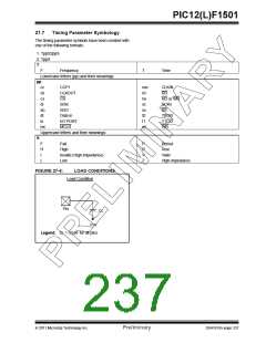
FIGURE 27-4:
LOAD CONDITIONS
Load Condition
Pin
CL
VSS
Legend: CL = 50 pF for all pins
2011 Microchip Technology Inc.
Preliminary
DS41615A-page 237

 MICROCHIP [ MICROCHIP ]