PIC12(L)F1501
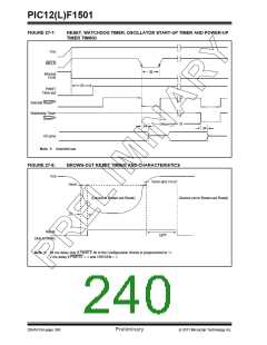
TABLE 27-4: RESET, WATCHDOG TIMER, OSCILLATOR START-UP TIMER, POWER-UP TIMER
AND BROWN-OUT RESET PARAMETERS
Standard Operating Conditions (unless otherwise stated)
Operating Temperature -40°C TA +125°C
Param
No.
Sym.
TMCL
Characteristic
Min. Typ† Max. Units
Conditions
30
MCLR Pulse Width (low)
2
5
—
—
—
—
s VDD = 3.3-5V, -40°C to +85°C
s VDD = 3.3-5V
31
TWDTLP Low-Power Watchdog Timer
Time-out Period
10
16
27
ms VDD = 3.3V-5V,
1:16 Prescaler used
33*
34*
TPWRT Power-up Timer Period, PWRTE = 0 40
65
—
140
2.0
ms
TIOZ
I/O high-impedance from MCLR Low
or Watchdog Timer Reset
—
s
35
VBOR
Brown-out Reset Voltage: BORV = 0 2.55 2.70 2.85
V
PIC12(L)F1501
BORV = 1 2.30 2.40 2.55
V
V
PIC12F1501
PIC12LF1501
1.80 1.90 2.05
36*
37*
VHYST
Brown-out Reset Hysteresis
0
1
25
3
50
5
mV -40°C to +85°C
TBORDC Brown-out Reset DC Response
Time
s VDD VBOR
*
These parameters are characterized but not tested.
†
Data in “Typ” column is at 3.0V, 25°C unless otherwise stated. These parameters are for design guidance
only and are not tested.
Note 1: To ensure these voltage tolerances, VDD and VSS must be capacitively decoupled as close to the device as
possible. 0.1 F and 0.01 F values in parallel are recommended.
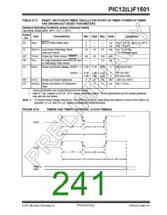
FIGURE 27-9:
TIMER0 AND TIMER1 EXTERNAL CLOCK TIMINGS
T0CKI
40
41
42
T1CKI
45
46
49
47
TMR0 or
TMR1
2011 Microchip Technology Inc.
Preliminary
DS41615A-page 241

 MICROCHIP [ MICROCHIP ]