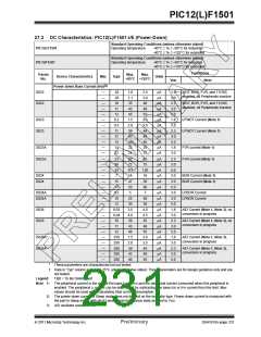
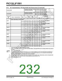
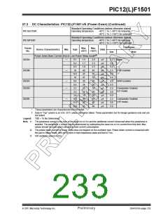
PIC12(L)F1501
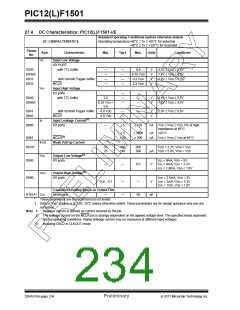
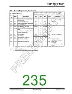
27.4 DC Characteristics: PIC12(L)F1501-I/E
Standard Operating Conditions (unless otherwise stated)
DC CHARACTERISTICS
Operating temperature -40°C TA +85°C for industrial
-40°C TA +125°C for extended
Param
No.
Sym.
Characteristic
Min.
Typ†
Max.
Units
Conditions
VIL
Input Low Voltage
I/O PORT:
D030
D030A
D031
D032
with TTL buffer
—
—
—
—
—
—
—
—
0.8
V
V
V
V
4.5V VDD 5.5V
0.15 VDD
0.2 VDD
0.2 VDD
1.8V VDD 4.5V
2.0V VDD 5.5V
with Schmitt Trigger buffer
MCLR
VIH
Input High Voltage
I/O ports:
—
—
—
—
—
—
D040
with TTL buffer
2.0
V
V
4.5V VDD 5.5V
1.8V VDD 4.5V
D040A
0.25 VDD +
0.8
D041
D042
with Schmitt Trigger buffer
MCLR
0.8 VDD
0.8 VDD
—
—
—
—
V
V
2.0V VDD 5.5V
(1)
IIL
Input Leakage Current
D060
I/O ports
—
—
± 5
± 125
nA
VSS VPIN VDD, Pin at high-
impedance at 85°C
± 5
± 1000
± 200
nA 125°C
D061
MCLR(2)
± 50
nA
A
V
VSS VPIN VDD at 85°C
IPUR
VOL
Weak Pull-up Current
D070*
25
25
100
140
200
300
VDD = 3.3V, VPIN = VSS
VDD = 5.0V, VPIN = VSS
(3)
Output Low Voltage
D080
D090
I/O ports
IOL = 8mA, VDD = 5V
IOL = 6mA, VDD = 3.3V
IOL = 1.8mA, VDD = 1.8V
—
—
0.6
(3)
VOH
Output High Voltage
I/O ports
IOH = 3.5mA, VDD = 5V
IOH = 3mA, VDD = 3.3V
IOH = 1mA, VDD = 1.8V
VDD - 0.7
—
—
—
V
Capacitive Loading Specs on Output Pins
All I/O pins
These parameters are characterized but not tested.
D101A* CIO
—
50
pF
*
†
Data in “Typ” column is at 3.0V, 25°C unless otherwise stated. These parameters are for design guidance only and are
not tested.
Note 1: Negative current is defined as current sourced by the pin.
2: The leakage current on the MCLR pin is strongly dependent on the applied voltage level. The specified levels represent
normal operating conditions. Higher leakage current may be measured at different input voltages.
3: Including OSC2 in CLKOUT mode.
DS41615A-page 234
Preliminary
2011 Microchip Technology Inc.

 MICROCHIP [ MICROCHIP ]