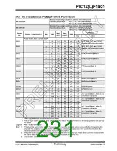
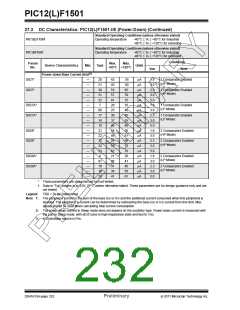
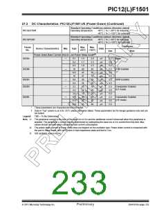
PIC12(L)F1501
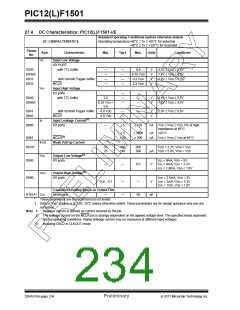
27.5 Memory Programming Requirements
Standard Operating Conditions (unless otherwise stated)
Operating temperature -40°C TA +125°C
DC CHARACTERISTICS
Param
Sym.
No.
Characteristic
Min.
Typ†
Max.
Units
Conditions
Program Memory Programming
Specifications
D110
D111
D112
D113
VIHH
IDDP
VBE
Voltage on MCLR/VPP pin
Supply Current during Programming
VDD for Bulk Erase
8.0
—
—
—
—
—
9.0
V
mA
V
(Note 2)
10
2.7
VDD max.
VDD max.
VPEW
VDD for Write or Row Erase
VDD min.
V
D114
IPPPGM Current on MCLR/VPP during Erase/
Write
—
1.0
—
mA
D115
IDDPGM Current on VDD during Erase/Write
Program Flash Memory
—
5.0
—
mA
D121
D122
D123
D124
EP
Cell Endurance
10K
VDD min.
—
—
—
2
—
VDD max.
2.5
E/W -40C to +85C (Note 1)
VPR
TIW
VDD for Read
V
Self-timed Write Cycle Time
ms
TRETD Characteristic Retention
—
40
—
Year Provided no other
specifications are violated
D125
EHEFC High-Endurance Flash Cell
100K
—
—
E/W 0C to +60C,
Lower byte,
Last 128 Addresses in Flash
Memory
†
Data in “Typ” column is at 3.0V, 25°C unless otherwise stated. These parameters are for design guidance only and are
not tested.
Note 1: Self-write and Block Erase.
2: Required only if single-supply programming is disabled.
2011 Microchip Technology Inc.
Preliminary
DS41615A-page 235

 MICROCHIP [ MICROCHIP ]