MCP3905/06
If an external voltage reference source is connected to
the REFIN/OUT pin, the external voltage will be used
as the reference for both current and voltage channel
ADCs. The voltage across the source resistor will then
be the difference between the internal and external
voltage. The allowed input range for the external volt-
age source goes from 2.2V to 2.6V for accurate mea-
surement error. A VREF value outside of this range will
cause additional heating and power consumption due
to the source resistor, which might affect measurement
error.
4.5
High-Pass Filters and Multiplier
The active (real) power value is extracted from the DC
instantaneous power. Therefore, any DC offset
component present on Channel 0 and Channel 1
affects the DC component of the instantaneous power
and will cause the real-power calculation to be
erroneous. In order to remove DC offset components
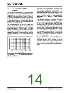
from the instantaneous power signal, a high-pass filter
has been introduced on each channel. Since the high-
pass filtering introduces phase delay, identical high-
pass filters are implemented on both channels. The
filters are clocked by the same digital signal, ensuring
a phase difference between the two channels of less
than one MCLK period. Under typical conditions
(MCLK = 3.58 MHz), this phase difference is less than
0.005°, with a line frequency of 50 Hz. The cut-off
frequency of the filter (4.45 Hz) has been chosen to
induce minimal gain error at typical line frequencies,
allowing sufficient settling time for the desired applica-
tions. The two high-pass filters can be disabled by
applying a logic ‘0’ to the HPF pin.
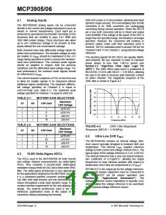
4.4
Power-On Reset (POR)
The MCP3905/06 contains an internal POR circuit that
monitors analog supply voltage AVDD during operation.
This circuit ensures correct device startup at system
power-up/power-down events. The POR circuit has
built-in hysteresis and a timer to give a high degree of
immunity to potential ripple and noise on the power
supplies, allowing proper settling of the power supply
during power-up. A 0.1 µF decoupling capacitor should
be mounted as close as possible to the AVDD pin,
providing additional transient immunity (see
Section 5.0 “Applications Information”).
0
-5
The threshold voltage is typically set at 4V, with a
tolerance of about ±5%. If the supply voltage falls below
this threshold, the MCP3905/06 will be held in a Reset
condition (equivalent to applying logic ‘0’ on the MCLR
pin). The typical hysteresis value is approximately
200 mV in order to prevent glitches on the power
supply.
-10
-15
-20
-25
-30
-35
-40
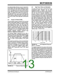
Once a power-up event has occurred, an internal timer
prevents the part from outputting any pulse for approx-
imately 1s (with MCLK = 3.58 MHz), thereby prevent-
ing potential metastability due to intermittent resets
caused by an unsettled regulated power supply.
Figure 4-3 illustrates the different conditions for a
power-up and a power-down event in the typical
conditions.
0.1
1
10
100
1000
Frequency (Hz)
FIGURE 4-4:
(MCLK = 3.58 MHz).
HPF Magnitude Response
The multiplier output gives the product of the two high-
pass-filtered channels, corresponding to instantaneous
active (real) power. Multiplying two sine wave signals
by the same ω frequency gives a DC component and a
2ω component. The instantaneous power signal con-
tains the active (real) power of its DC component, while
also containing 2ω components coming from the line
frequency multiplication. These 2ω components come
for the line frequency (and its harmonics) and must be
removed in order to extract the real-power information.
This is accomplished using the low-pass filter and DTF
converter.
AV
DD
5V
4.2V
4V
1s
0V
Time
NO
PULSE
OUT
PROPER
OPERATION
DEVICE
MODE
RESET
RESET
FIGURE 4-3:
Power-on Reset Operation.
© 2007 Microchip Technology Inc.
DS21948D-page 13

 MICROCHIP [ MICROCHIP ]