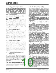
MCP3905/06
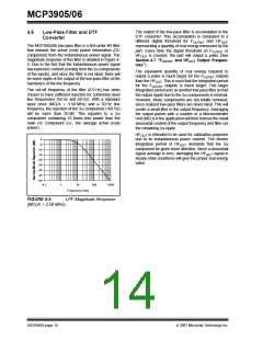
3.5
Voltage Channel (CH1-,CH1+)
3.11 Oscillator (OSC1, OSC2)
OSC1 and OSC2 provide the master clock for the
device. A resonant crystal or clock source with a similar
sinusoidal waveform must be placed across these pins
to ensure proper operation. The typical clock frequency
specified is 3.579545 MHz. However, the clock
frequency can be with the range of 1 MHz to 4 MHz
without disturbing measurement error. Appropriate
load capacitance should be connected to these pins for
proper operation.
CH1- and CH1+ are the fully differential analog voltage
input channels for the voltage measurement. The linear
and specified region of these channels have a
maximum differential voltage of ±660mV and a
maximum absolute voltage of ±1V, with respect to
AGND. Up to ±6V can be applied to these pins without
the risk of permanent damage.
Refer to Section 1.0 “Electrical Characteristics”.
A full-swing, single-ended clock source may be
connected to OSC1 with proper resistors in series to
ensure no ringing of the clock source due to fast
transient edges.
3.6
Master Clear (MCLR)
MCLR controls the reset for both delta-sigma ADCs, all
digital registers, the SINC filters for each channel and
all accumulators post multiplier. A logic ‘0’ resets all
registers and holds both ADCs in a Reset condition.
The charge stored in both ADCs is flushed and their
output is maintained to 0x0000h. The only block
consuming power on the digital power supply during
Reset is the oscillator circuit.
3.12 Negative Power Output Logic Pin
(NEG)
NEG detects the phase difference between the two
channels and will go to a logic ‘1’ state when the phase
difference is greater than 90° (i.e., when the measured
active (real) power is negative). The output state is syn-
chronous with the rising-edge of HFOUT and maintains
the logic ‘1’ until the active (real) power becomes posi-
tive again and HFOUT shows a pulse.
3.7
Reference (REFIN/OUT)
REFIN/OUT is the output for the internal 2.4V
reference. This reference has a typical temperature
coefficient of 15 ppm/°C and a tolerance of ±2%. In
addition, an external reference can also be used by
applying voltage to this pin within the specified range.
REFIN/OUT requires appropriate bypass capacitors to
AGND, even when using the internal reference only.
Refer to Section 5.0 “Applications Information”.
3.13 Ground Connection (D
)
GND
DGND is the ground connection to the internal digital
circuitry (SINC filters, multiplier, HPF, LPF, Digital-to-
Frequency (DTF) converter and oscillator). To ensure
accuracy and noise cancellation, DGND must be
connected to the same ground as AGND, preferably
with a star connection. If a digital ground plane is
available, it is recommended that this device be tied to
this plane of the PCB. This plane should also reference
all other digital circuitry in the system.
3.8
Analog Ground (A
)
GND
AGND is the ground connection to the internal analog
circuitry (ADCs, PGA, band gap reference, POR). To
ensure accuracy and noise cancellation, this pin must
be connected to the same ground as DGND, preferably
with a star connection. If an analog ground plane is
available, it is recommended that this device be tied to
this plane of the Printed Circuit Board (PCB). This
plane should also reference all other analog circuitry in
the system.
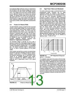
3.14 High-Frequency Output (HF
)
OUT
HFOUT is the high-frequency output of the device and
supplies the instantaneous real-power information. The
output is a periodic pulse output, with its period propor-
tional to the measured active (real) power, and to the
HFC constant defined by F0, F1 and F2 pin logic states.
This output is the preferred output for calibration due to
faster output frequencies, giving smaller calibration
times. Since this output gives instantaneous active
(real) power, the 2ω ripple on the output should be
noted. However, the average period will show minimal
drift.
3.9
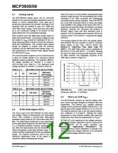
Frequency Control Logic Pins
(F2, F1, F0)
F2, F1 and F0 select the high-frequency output and
low-frequency output pin ranges by changing the
value of the constants FC and HFC used in the device
transfer function. FC and HFC are the frequency
constants that define the period of the output pulses
for the device.
3.15 Frequency Output (F
, F
)
OUT0 OUT1
FOUT0 and FOUT1 are the frequency outputs of the
device that supply the average real-power information.
The outputs are periodic pulse outputs, with its period
proportional to the measured active (real) power, and to
the Fc constant, defined by the F0 and F1 pin logic
states. These pins include high-output drive capability
for direct use of electromechanical counters and 2-
phase stepper motors. Since this output supplies
average active (real) power, any 2ω ripple on the output
pulse period is minimal.
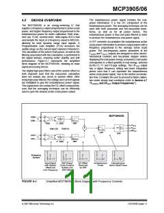
3.10 Gain Control Logic Pins (G1, G0)
G1 and G0 select the PGA gain on Channel 0 from
three different values: 1, 8 and 16.
DS21948D-page 10
© 2007 Microchip Technology Inc.

 MICROCHIP [ MICROCHIP ]