MCP3905/06
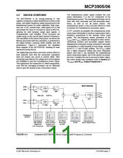
3.0
PIN DESCRIPTIONS
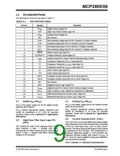
The descriptions of the pins are listed in Table 3-1.
TABLE 3-1:
Pin No.
PIN FUNCTION TABLE
Symbol
Function
1
DVDD
HPF
Digital Power Supply Pin
High-Pass Filters Control Logic Pin
2
3
AVDD
NC
Analog Power Supply Pin
No Connect
4
5
CH0+
CH0-
CH1-
CH1+
MCLR
REFIN/OUT
AGND
F2
Non-Inverting Analog Input Pin for Channel 0 (Current Channel)
Inverting Analog Input Pin for Channel 0 (Current Channel)
Inverting Analog Input Pin for Channel 1 (Voltage Channel)
Non-Inverting Analog Input Pin for Channel 1 (Voltage Channel)
Master Clear Logic Input Pin
6
7
8
9
10
11
12
13
14
15
16
17
18
19
20
21
22
23
24
Voltage Reference Input/Output Pin
Analog Ground Pin, Return Path for internal analog circuitry
Frequency Control for HFOUT Logic Input Pin
Frequency Control for FOUT0/1 Logic Input Pin
Frequency Control for FOUT0/1 Logic Input Pin
Gain Control Logic Input Pin
F1
F0
G1
G0
Gain Control Logic Input Pin
OSC1
OSC2
NC
Oscillator Crystal Connection Pin or Clock Input Pin
Oscillator Crystal Connection Pin or Clock Output Pin
No Connect
NEG
DGND
HFOUT
FOUT1
FOUT0
Negative Power Logic Output Pin
Digital Ground Pin, Return Path for Internal Digital Circuitry
High-Frequency Logic Output Pin (Intended for Calibration)
Differential Mechanical Counter Logic Output Pin
Differential Mechanical Counter Logic Output Pin
3.1
Digital V (DV
)
3.3
Analog V (AV
)
DD
DD
DD
DD
AVDD is the power supply pin for the analog circuitry
within the MCP3905/06.
DVDD is the power supply pin for the digital circuitry
within the MCP3905/06.
AVDD requires appropriate bypass capacitors and
should be maintained to 5V ±10% for specified
operation. Please refer to Section 5.0 “Applications
Information”.
DVDD requires appropriate bypass capacitors and
should be maintained to 5V ±10% for specified
operation. Please refer to Section 5.0 “Applications
Information”.
3.4
Current Channel (CH0-, CH0+)
3.2
High-Pass Filter Input Logic Pin
(HPF)
CH0- and CH0+ are the fully differential analog voltage
input channels for the current measurement, containing
a PGA for small-signal input, such as shunt current-
sensing. The linear and specified region of this channel
is dependant on the PGA gain. This corresponds to a
maximum differential voltage of ±470 mV/GAIN and
maximum absolute voltage, with respect to AGND, of
±1V. Up to ±6V can be applied to these pins without the
risk of permanent damage.
HPF controls the state of the high-pass filter in both
input channels. A logic ‘1’ enables both filters,
removing any DC offset coming from the system or the
device. A logic ‘0’ disables both filters, allowing DC
voltages to be measured.
Refer to Section 1.0 “Electrical Characteristics”.
© 2007 Microchip Technology Inc.
DS21948D-page 9

 MICROCHIP [ MICROCHIP ]