MCP3905/06
Both ADCs have a 16-bit resolution, allowing wide input
dynamic range sensing. The oversampling ratio of both
converters is 64. Both converters are continuously
converting during normal operation. When the MCLR
pin is low, both converters will be in Reset and output
code 0x0000h. If the voltage at the inputs of the ADC is
larger than the specified range, the linearity is no longer
specified. However, the converters will continue to
produce output codes until their saturation point is
reached. The DC saturation point is around 700 mV for
Channel 0 and 1V for Channel 1, using internal voltage
reference.
4.1
Analog Inputs
The MCP3905/06 analog inputs can be connected
directly to the current and voltage transducers (such as
shunts or current transformers). Each input pin is
protected by specialized Electrostatic Discharge (ESD)
structures that are certified to pass 5 kV HBM and
500V MM contact charge. These structures also allow
up to ±6V continuous voltage to be present at their
inputs without the risk of permanent damage.
Both channels have fully differential voltage inputs for
better noise performance. The absolute voltage at each
pin relative to AGND should be maintained in the ±1V
range during operation in order to ensure the measure-
ment error performance. The common mode signals
should be adapted to respect both the previous
conditions and the differential input voltage range. For
best performance, the common mode signals should
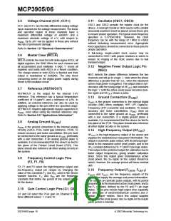
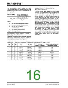
The clocking signals for the ADCs are equally distrib-
uted between the two channels in order to minimize
phase delays to less than 1 MCLK period (see
Section 3.2 “High-Pass Filter Input Logic Pin
(HPF)”). The SINC filters main notch is positioned at
MCLK/256 (14 kHz with MCLK = 3.58 MHz), allowing
the user to be able to measure wide harmonic content
on either channel. The magnitude response of the
SINC filter is shown in Figure 4-2.
be referenced to AGND
.
The current channel comprises a PGA on the front-end
to allow for smaller signals to be measured without
additional signal conditioning. The maximum differen-
tial voltage specified on Channel 0 is equal to
±470 mV/Gain (see Table 4-1). The maximum peak
voltage specified on Channel 1 is equal to ±660 mV.
0
-20
-40
TABLE 4-1:
MCP3905 GAIN SELECTIONS
-60
Maximum
CH0 Gain
G1
G0
CH0 Voltage
-80
0
0
1
1
0
1
0
1
1
2
±470 mV
±235 mV
±60 mV
±30 mV
-100
-120
8
0
5
10
15
20
25
30
16
Frequency (kHz)
TABLE 4-2:
MCP3906 GAIN SELECTIONS
FIGURE 4-2:
Response (MCLK = 3.58 MHz).
SINC Filter Magnitude
Maximum
CH0 Gain
G1
G0
CH0 Voltage
0
0
1
1
0
1
0
1
1
32
8
±470 mV
±15 mV
±60 mV
±30 mV
4.3 Ultra-Low Drift V
REF
The MCP3905/06 contains an internal voltage refer-
ence source specially designed to minimize drift over
temperature. This internal VREF supplies reference
voltage to both current and voltage channel ADCs. The
typical value of this voltage reference is 2.4V, ±100 mV.
The internal reference has a very low typical tempera-
ture coefficient of ±15 ppm/°C, allowing the output
frequencies to have minimal variation with respect to
temperature since they are proportional to (1/VREF)².
16
4.2
16-Bit Delta-Sigma ADCs
The ADCs used in the MCP3905/06 for both current
and voltage channel measurements are delta-sigma
ADCs. They comprise a second-order, delta-sigma
modulator using a multi-bit DAC and a third-order SINC
filter. The delta-sigma architecture is very appropriate
for the applications targeted by the MCP3905, because
it is a waveform-oriented converter architecture that
can offer both high linearity and low distortion perfor-
mance throughout a wide input dynamic range. It also
creates minimal requirements for the anti-aliasing filter
design. The multi-bit architecture used in the ADC
minimizes quantization noise at the output of the
converters without disturbing the linearity.
REFIN/OUT is the output pin for the voltage reference.
Appropriate bypass capacitors must be connected to
the REFIN/OUT pin for proper operation (see
Section 5.0 “Applications Information”). The
voltage reference source impedance is typically 4 kΩ,
which enables this voltage reference to be overdriven
by an external voltage reference source.
DS21948D-page 12
© 2007 Microchip Technology Inc.

 MICROCHIP [ MICROCHIP ]