MCP23018/MCP23S18
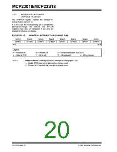
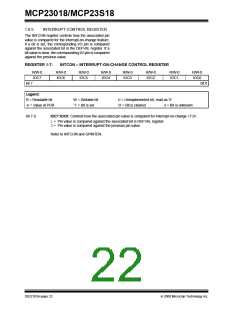
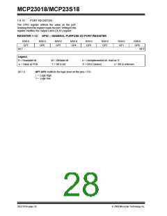
REGISTER 1-8:
IOCON – I/O EXPANDER CONFIGURATION REGISTER
R/W-0
BANK
R/W-0
R/W-0
U-0
-
U-0
-
R/W-0
ODR
R/W-0
R/W-0
INTCC
SEQOP
MIRROR
INTPOL
bit 7
bit 0
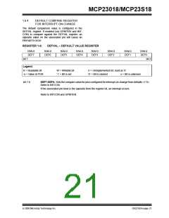
Legend:
R = Readable bit
-n = Value at POR
W = Writable bit
‘1’ = Bit is set
U = Unimplemented bit, read as ‘0’
‘0’ = Bit is cleared x = Bit is unknown
bit 7
bit 6
bit 5
BANK: Controls how the registers are addressed (see Figure 1-4 and Figure 1-5)
1 = The registers associated with each port are separated into different banks
0 = The registers are in the same bank (addresses are sequential)
MIRROR: INT pins mirror bit
1 = The INT pins are internally connected in a wired OR configuration
0 = The INT pins are not connected. INTA is associated with Port A and INTB is associated with Port B
SEQOP: Sequential Operation mode bit.
1= Sequential operation disabled, address pointer does not increment.
0= Sequential operation enabled, address pointer increments.
bit 4
bit 3
bit 2
Unimplemented: Reads as 0
Unimplemented: Reads as 0
ODR: Configures the INT pin as an open-drain output.
1= Open-drain output (overrides the INTPOL bit).
0= Active driver output (INTPOL bit sets the polarity).
bit 1
bit 0
INTPOL: Sets the polarity of the INT output pin.
1= Active-high.
0= Active-low.
INTCC: Interrupt Clearing Control
1 = Reading INTCAP register clears the interrupt
0 = Reading GPIO register clears the interrupt
DS22103A-page 24
© 2008 Microchip Technology Inc.

 MICROCHIP [ MICROCHIP ]