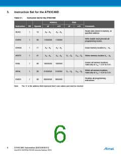
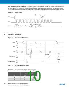
5.
Instruction Set for the AT93C46D
Table 5-1.
Instruction Set for the AT93C46D
Address
Data
Instruction
SB
Opcode
x8
x16
x8
x16
Comments
Reads data stored in memory, at
specified address.
READ
1
10
A6 – A0
A5 – A0
Write enable must precede all
programming modes.
EWEN
ERASE
WRITE
ERAL
1
1
1
1
1
1
00
11
01
00
00
00
11XXXXX
A6 – A0
11XXXX
A5 – A0
Erase memory location An – A0.
Writes memory location An – A0.
A6 – A0
A5 – A0
D7 – D0
D15 – D0
Erases all memory locations.
Valid only at VCC = 4.5V to 5.5V.
10XXXXX
01XXXXX
00XXXXX
10XXXX
01XXXX
00XXXX
Writes all memory locations.
Valid only at VCC = 4.5V to 5.5V.
WRAL
EWDS
D7 – D0
D15 – D0
Disables all programming.
instructions.
Note:
The ‘X’ in the address field represent don’t care values and must be clocked.
6
AT93C46D Automotive [DATASHEET]
Atmel-8674C-SEEPROM-AT93C46D-Automotive-Datasheet_102014

 MICROCHIP [ MICROCHIP ]