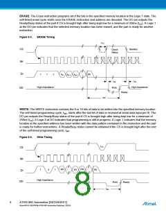
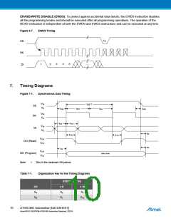
ERASE/WRITE DISABLE (EWDS): To protect against accidental data disturb, the EWDS instruction disables
all the programming modes and should be executed after all programming operations. The operation of the
READ instruction is independent of both the EWEN and EWDS instructions and can be executed at any time.
Figure 6-7.
EWDS Timing
tCS
CS
SK
DI
...
0
0
0
1
0
7.
Timing Diagrams
Figure 7-1.
Synchronous Data Timing
1µs(1)
VIH
CS
VIL
tSKH
tCSS
tSKL
tCSH
VIH
VIL
SK
DI
tDIS
tDIH
VIH
VIL
tDF
tPD0
tPD1
VOH
VOL
DO (Read)
tDF
tSV
VOH
VOL
DO (Program)
Status Valid
Note:
1. This is the minimum SK period.
Table 7-1.
Organization Key for the Timing Diagrams
AT93C46D (1K)
I/O
AN
DN
x 8
A6
x 16
A5
D7
D15
10
AT93C46D Automotive [DATASHEET]
Atmel-8674C-SEEPROM-AT93C46D-Automotive-Datasheet_102014

 MICROCHIP [ MICROCHIP ]