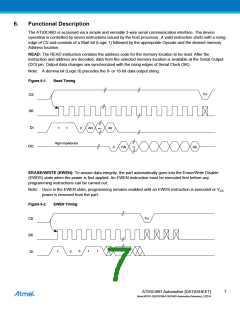
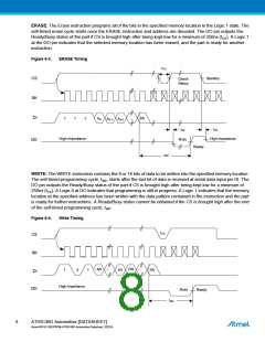
ERASE: The Erase instruction programs all of the bits in the specified memory location to the Logic 1 state. The
self-timed erase cycle starts once the ERASE instruction and address are decoded. The DO pin outputs the
Ready/Busy status of the part if CS is brought high after being kept low for a minimum of 250ns (tCS). A Logic 1
at the DO pin indicates that the selected memory location has been erased, and the part is ready for another
instruction.
Figure 6-3.
ERASE Timing
tCS
Standby
CS
SK
DI
Check
Status
A0
1
1
1
AN
...
AN-1 AN-2
tDF
High-impedance
tSV
High-impedance
Busy
DO
Ready
tWP
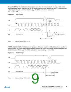
WRITE: The WRITE instruction contains the 8 or 16 bits of data to be written into the specified memory location.
The self-timed programming cycle, tWP, starts after the last bit of data is received at serial data input pin DI. The
DO pin outputs the Ready/Busy status of the part if CS is brought high after being kept low for a minimum of
250ns (tCS). A Logic 0 at DO indicates that programming is still in progress. A Logic 1 indicates that the memory
location at the specified address has been written with the data pattern contained in the instruction and the part
is ready for further instructions. A Ready/Busy status cannot be obtained if the CS is brought high after the end
of the self-timed programming cycle, tWP
.
Figure 6-4.
Write Timing
tCS
CS
SK
...
...
AN
DN
1
0
1
A0
D0
DI
High-impedance
DO
Busy
Ready
tWP
8
AT93C46D Automotive [DATASHEET]
Atmel-8674C-SEEPROM-AT93C46D-Automotive-Datasheet_102014

 MICROCHIP [ MICROCHIP ]