1.
Pin Configurations and Pinouts
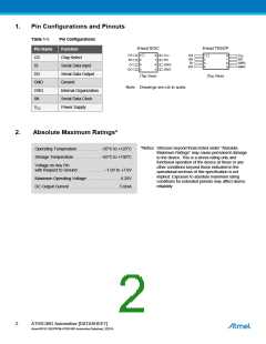
Table 1-1.
Pin Configurations
8-lead SOIC
8-lead TSSOP
Pin Name
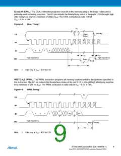
CS
Function
1
2
3
4
8
7
6
5
CS
SK
DI
VCC
DC
ORG
GND
CS
SK
DI
VCC
DC
ORG
GND
1
2
3
4
8
7
6
5
Chip Select
DI
Serial Data Input
Serial Data Output
Ground
DO
DO
DO
(Top View)
(Top View)
GND
ORG
SK
Note: Drawings are not to scale.
Internal Organization
Serial Data Clock
Power Supply
VCC
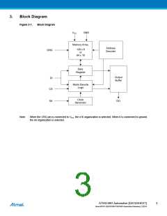
2.
Absolute Maximum Ratings*
*Notice: Stresses beyond those listed under “Absolute
Operating Temperature 55C to +125C
Storage Temperature65C to +150C
Maximum Ratings” may cause permanent damage
to the device. This is a stress rating only and
functional operation of the device at these or any
other conditions beyond those indicated in the
operational sections of this specification is not
implied. Exposure to absolute maximum rating
conditions for extended periods may affect device
reliability
Voltage on Any Pin
with Respect to Ground1.0V to +7.0V
Maximum Operating Voltage . . . . . . . . . . . . . . . 6.25V
DC Output Current . . . . . . . . . . . . . . . . . . . . . . .5.0mA
2
AT93C46D Automotive [DATASHEET]
Atmel-8674C-SEEPROM-AT93C46D-Automotive-Datasheet_102014

 MICROCHIP [ MICROCHIP ]