6.
Functional Description
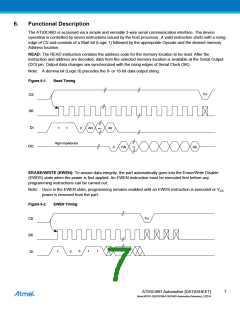
The AT93C46D is accessed via a simple and versatile 3-wire serial communication interface. The device
operation is controlled by seven instructions issued by the host processor. A valid instruction starts with a rising
edge of CS and consists of a Start bit (Logic 1) followed by the appropriate Opcode and the desired memory
Address location.
READ: The READ instruction contains the address code for the memory location to be read. After the
instruction and address are decoded, data from the selected memory location is available at the Serial Output
(DO) pin. Output data changes are synchronized with the rising edges of Serial Clock (SK).
Note: A dummy bit (Logic 0) precedes the 8- or 16-bit data output string.
Figure 6-1.
Read Timing
tCS
CS
SK
DI
1
1
0
AN
A0
High-impedance
DO
0
DN
D0
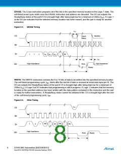
ERASE/WRITE (EWEN): To assure data integrity, the part automatically goes into the Erase/Write Disable
(EWDS) state when the power is first applied. An EWEN instruction must be executed first before any
programming instructions can be carried out.
Note: Once in the EWEN state, programming remains enabled until an EWDS instruction is executed or VCC
power is removed from the part.
Figure 6-2.
EWEN Timing
tCS
CS
SK
DI
...
0
1
1
1
0
AT93C46D Automotive [DATASHEET]
Atmel-8674C-SEEPROM-AT93C46D-Automotive-Datasheet_102014
7

 MICROCHIP [ MICROCHIP ]