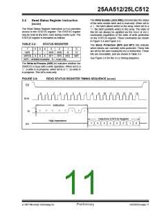
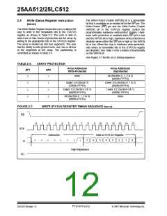
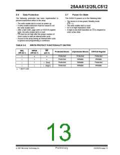
25AA512/25LC512
2.9
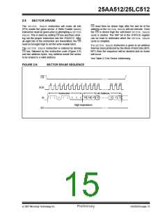
SECTOR ERASE
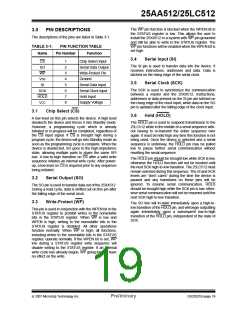
The SECTOR ERASE instruction will erase all bits
(FFh) inside the given sector. A Write Enable (WREN)
instruction must be given prior to attempting a SECTOR
ERASE. This is done by setting CS low and then clock-
ing out the proper instruction into the 25XX512. After
all eight bits of the instruction are transmitted, the CS
must be brought high to set the write enable latch.
CS must then be driven high after the last bit of the
address or the SECTOR ERASEwill not execute. Once
the CS is driven high the self-timed SECTOR ERASE
cycle is started. The WIP bit in the STATUS register
can be read to determine when the SECTOR ERASE
cycle is complete.
If a SECTOR ERASEinstruction is given to an address
that has been protected by the Block Protect bits (BP0,
BP1) then the sequence will be aborted and no erase
will occur.
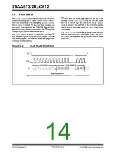
The SECTOR ERASE instruction is entered by driving
CS low, followed by the instruction code (Figure 2-9)
and two address bytes. Any address inside the sector
to be erased is a valid address.
See Table 2-3 for Sector Addressing.
FIGURE 2-9:
SECTOR ERASE SEQUENCE
CS
SCK
SI
0
1
2
3
4
5
6
7
8
9 10 11
21 22 23
Instruction
16-bit Address
15 14 13 12
1
1
0
1
1
0
0
0
2
1
0
High-Impedance
SO
© 2007 Microchip Technology Inc.
Preliminary
DS22021B-page 15

 MICROCHIP [ MICROCHIP ]