25AA512/25LC512
The WP pin function is blocked when the WPEN bit in
the STATUS register is low. This allows the user to
install the 25XX512 in a system with WP pin grounded
and still be able to write to the STATUS register. The
WP pin functions will be enabled when the WPEN bit is
set high.
3.0
PIN DESCRIPTIONS
The descriptions of the pins are listed in Table 3-1.
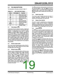
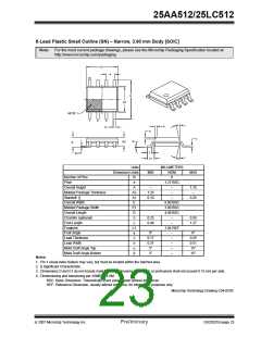
TABLE 3-1:
Name
PIN FUNCTION TABLE
Pin Number
Function
3.4
Serial Input (SI)
CS
SO
1
2
3
4
5
6
7
8
Chip Select Input
Serial Data Output
Write-Protect Pin
Ground
The SI pin is used to transfer data into the device. It
receives instructions, addresses and data. Data is
latched on the rising edge of the serial clock.
WP
VSS
SI
3.5
Serial Clock (SCK)
Serial Data Input
Serial Clock Input
Hold Input
The SCK is used to synchronize the communication
between a master and the 25XX512. Instructions,
addresses or data present on the SI pin are latched on
the rising edge of the clock input, while data on the SO
pin is updated after the falling edge of the clock input.
SCK
HOLD
VCC
Supply Voltage
3.1
Chip Select (CS)
3.6
Hold (HOLD)
A low level on this pin selects the device. A high level
deselects the device and forces it into Standby mode.
However, a programming cycle which is already
initiated or in progress will be completed, regardless of
the CS input signal. If CS is brought high during a
program cycle, the device will go into Standby mode as
soon as the programming cycle is complete. When the
device is deselected, SO goes to the high-impedance
state, allowing multiple parts to share the same SPI
bus. A low-to-high transition on CS after a valid write
sequence initiates an internal write cycle. After power-
up, a low level on CS is required prior to any sequence
being initiated.
The HOLD pin is used to suspend transmission to the
25LC512 while in the middle of a serial sequence with-
out having to re-transmit the entire sequence over
again. It must be held high any time this function is not
being used. Once the device is selected and a serial
sequence is underway, the HOLD pin may be pulled
low to pause further serial communication without
resetting the serial sequence.
The HOLD pin should be brought low while SCK is low,
otherwise the HOLD function will not be invoked until
the next SCK high-to-low transition. The 25LC512 must
remain selected during this sequence. The SI and SCK
levels are “don’t cares” during the time the device is
paused and any transitions on these pins will be
ignored. To resume serial communication, HOLD
should be brought high while the SCK pin is low, other-
wise serial communication will not be resumed until the
next SCK high-to-low transition.
3.2
Serial Output (SO)
The SO pin is used to transfer data out of the 25XX512.
During a read cycle, data is shifted out on this pin after
the falling edge of the serial clock.
3.3
Write-Protect (WP)
The SO line will tri-state immediately upon a high-to-
low transition of the HOLD pin, and will begin outputting
again immediately upon a subsequent low-to-high
transition of the HOLD pin, independent of the state of
SCK.
This pin is used in conjunction with the WPEN bit in the
STATUS register to prohibit writes to the nonvolatile
bits in the STATUS register. When WP is low and
WPEN is high, writing to the nonvolatile bits in the
STATUS register is disabled. All other operations
function normally. When WP is high, all functions,
including writes to the nonvolatile bits in the STATUS
register, operate normally. If the WPEN bit is set, WP
low during a STATUS register write sequence will
disable writing to the STATUS register. If an internal
write cycle has already begun, WP going low will have
no effect on the write.
© 2007 Microchip Technology Inc.
Preliminary
DS22021B-page 19

 MICROCHIP [ MICROCHIP ]