PIC12CE67X
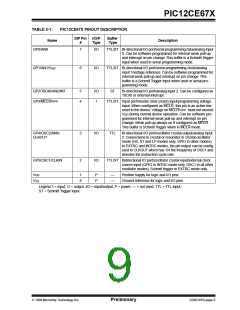
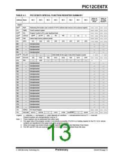
TABLE 3-1:
PIC12CE67X PINOUT DESCRIPTION
DIP Pin
#
I/O/P
Type
Buffer
Type
Name
Description
GP0/AN0
7
6
I/O
I/O
TTL/ST Bi-directional I/O port/serial programming data/analog input
0. Can be software programmed for internal weak pull-up
and interrupt on pin change.This buffer is a Schmitt Trigger
input when used in serial programming mode.
GP1/AN1/VREF
TTL/ST Bi-directional I/O port/serial programming clock/analog
input 1/voltage reference. Can be software programmed for
internal weak pull-up and interrupt on pin change. This
buffer is a Schmitt Trigger input when used in serial pro-
gramming mode.
GP2/T0CKI/AN2/INT
GP3/MCLR/VPP
5
4
I/O
I
ST
Bi-directional I/O port/analog input 2. Can be configured as
T0CKI or external interrupt.
TTL/ST Input port/master clear (reset) input/programming voltage
input. When configured as MCLR, this pin is an active low
reset to the device.Voltage on MCLR/VPP must not exceed
VDD during normal device operation. Can be software pro-
grammed for internal weak pull-up and interrupt on pin
change. Weak pull-up always on if configured as MCLR .
This buffer is Schmitt Trigger when in MCLR mode.
GP4/OSC2/AN3/
CLKOUT
3
2
I/O
I/O
TTL
Bi-directional I/O port/oscillator crystal output/analog input
3. Connections to crystal or resonator in crystal oscillator
mode (HS, XT and LP modes only, GPIO in other modes).
In EXTRC and INTRC modes, the pin output can be config-
ured to CLKOUT which has 1/4 the frequency of OSC1 and
denotes the instruction cycle rate.
GP5/OSC1/CLKIN
TTL/ST Bidirectional IO port/oscillator crystal input/external clock
source input (GPIO in INTRC mode only, OSC1 in all other
oscillator modes). Schmitt trigger in EXTRC mode only.
VDD
VSS
1
8
P
P
—
—
Positive supply for logic and I/O pins
Ground reference for logic and I/O pins
Legend: I = input, O = output, I/O = input/output, P = power, — = not used, TTL = TTL input,
ST = Schmitt Trigger input
1998 Microchip Technology Inc.
Preliminary
DS40181B-page 9

 MICROCHIP [ MICROCHIP ]