PIC12CE67X
3.1
Clocking Scheme/Instruction Cycle
3.2
Instruction Flow/Pipelining
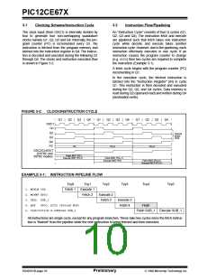
The clock input (from OSC1) is internally divided by
four to generate four non-overlapping quadrature
clocks namely Q1, Q2, Q3 and Q4. Internally, the pro-
gram counter (PC) is incremented every Q1, the
instruction is fetched from the program memory and
latched into the instruction register in Q4. The instruc-
tion is decoded and executed during the following Q1
through Q4. The clocks and instruction execution flow
is shown in Figure 3-2.
An “Instruction Cycle” consists of four Q cycles (Q1,
Q2, Q3 and Q4). The instruction fetch and execute
are pipelined such that fetch takes one instruction
cycle while decode and execute takes another
instruction cycle. However, due to the pipelining, each
instruction effectively executes in one cycle. If an
instruction causes the program counter to change
(e.g. GOTO) then two cycles are required to complete
the instruction (Example 3-1).
A fetch cycle begins with the program counter (PC)
incrementing in Q1.
In the execution cycle, the fetched instruction is
latched into the “Instruction Register" (IR) in cycle
Q1. This instruction is then decoded and executed
during the Q2, Q3, and Q4 cycles. Data memory is
read during Q2 (operand read) and written during Q4
(destination write).
FIGURE 3-2: CLOCK/INSTRUCTION CYCLE
Q2
Q3
Q4
Q2
Q3
Q4
Q2
Q3
Q4
Q1
Q1
Q1
OSC1
Q1
Q2
Q3
Internal
phase
clock
Q4
PC
PC
PC+1
PC+2
OSC2/CLKOUT
(EXTRC and
INTRC modes)
Fetch INST (PC)
Execute INST (PC-1)
Fetch INST (PC+1)
Execute INST (PC)
Fetch INST (PC+2)
Execute INST (PC+1)
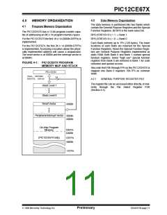
EXAMPLE 3-1: INSTRUCTION PIPELINE FLOW
Tcy0
Tcy1
Tcy2
Tcy3
Tcy4
Tcy5
1. MOVLW 55h
2. MOVWF GPIO
3. CALL SUB_1
Fetch 1
Execute 1
Fetch 2
Execute 2
Fetch 3
Execute 3
Fetch 4
4. BSF
GPIO, BIT3 (Forced NOP)
Flush
5. Instruction @ address SUB_1
Fetch SUB_1 Execute SUB_1
All instructions are single cycle, except for any program branches.These take two cycles since the fetch instruc-
tion is “flushed” from the pipeline while the new instruction is being fetched and then executed.
DS40181B-page 10
Preliminary
1998 Microchip Technology Inc.

 MICROCHIP [ MICROCHIP ]