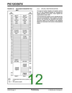
PIC12CE67X
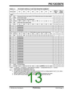
TABLE 4-1:
PIC12CE67X SPECIAL FUNCTION REGISTER SUMMARY
Value on
Power-on
Reset
Value on
all other
Resets(3)
Address Name
Bit 7
Bit 6
Bit 5
Bit 4
Bit 3
Bit 2
Bit 1
Bit 0
Bank 0
00h(1)
01h
INDF
TMR0
PCL
STATUS
FSR
GPIO
—
Addressing this location uses contents of FSR to address data memory (not a physical register)
Timer0 module’s register
0000 0000 0000 0000
xxxx xxxx uuuu uuuu
0000 0000 0000 0000
0001 1xxx 000q quuu
xxxx xxxx uuuu uuuu
11xx xxxx 11uu uuuu
02h(1)
03h(1)
04h(1)
05h
Program Counter's (PC) Least Significant Byte
IRP(4)
RP1(4)
RP0
TO
PD
Z
DC
C
Indirect data memory address pointer
SCL
SDA
GP5
GP4
GP3
GP2
GP1
GP0
06h
Unimplemented
Unimplemented
Unimplemented
Unimplemented
—
—
—
—
—
—
—
—
—
07h
—
08h
—
09h
—
0Ah(1,2) PCLATH
—
—
T0IE
—
Write Buffer for the upper 5 bits of the Program Counter
---0 0000 ---0 0000
0000 000x 0000 000u
-0-- ---- -0-- ----
0Bh(1)
0Ch
0Dh
0Eh
0Fh
10h
11h
12h
13h
14h
15h
16h
17h
18h
19h
1Ah
1Bh
1Ch
1Dh
1Eh
1Fh
INTCON
GIE
—
PEIE
ADIF
INTE
—
GPIE
—
T0IF
—
INTF
—
GPIF
—
PIR1
—
Unimplemented
Unimplemented
Unimplemented
Unimplemented
Unimplemented
Unimplemented
Unimplemented
Unimplemented
Unimplemented
Unimplemented
Unimplemented
Unimplemented
Unimplemented
Unimplemented
Unimplemented
Unimplemented
Unimplemented
A/D Result Register
—
—
—
—
—
—
—
—
—
—
—
—
—
—
—
—
—
—
—
—
—
—
—
—
—
—
—
—
—
—
—
—
—
—
—
—
—
—
—
—
—
—
—
—
—
—
—
—
—
—
ADRES
ADCON0
xxxx xxxx uuuu uuuu
0000 0000 0000 0000
ADCS1
ADCS0
r
CHS1
CHS0
GO/DONE
r
ADON
Legend: x= unknown, u= unchanged, q= value depends on condition, - = unimplemented read as '0', r = reserved.
Shaded locations are unimplemented, read as ‘0’.
Note 1: These registers can be addressed from either bank.
2: The upper byte of the program counter is not directly accessible. PCLATH is a holding register for the PC<12:8> whose
contents are transferred to the upper byte of the program counter.
3: Other (non power-up) resets include external reset through MCLR and Watchdog Timer Reset.
4: The IRP and RP1 bits are reserved on the PIC12CE67X, always maintain these bits clear.
1998 Microchip Technology Inc.
Preliminary
DS40181B-page 13

 MICROCHIP [ MICROCHIP ]