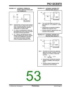
PIC12CE67X
The CLRWDT and SLEEP instructions clear the WDT
and the postscaler, if assigned to the WDT, and prevent
it from timing out early and generating a premature
device RESET condition.
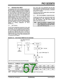
9.7
Watchdog Timer (WDT)
The WatchdogTimer is a free running on-chip RC oscil-
lator which does not require any external components.
This RC oscillator is separate from the RC oscillator of
the OSC1/CLKIN pin. That means that the WDT will
run, even if the clock on the OSC1/CLKIN and OSC2/
CLKOUT pins of the device has been stopped, for
example, by execution of a SLEEP instruction. During
normal operation, a WDT time-out generates a device
RESET (Watchdog Timer Reset). If the device is in
SLEEP mode, a WDT time-out causes the device to
wake-up and continue with normal operation (Watch-
dog Timer Wake-up). The WDT can be permanently
disabled by clearing configuration bit WDTE
(Section 9.1).
The TO bit in the STATUS register will be cleared upon
a Watchdog Timer time-out.
9.7.2
WDT PROGRAMMING CONSIDERATIONS
It should also be taken into account that under worst
case conditions (VDD = Min., Temperature = Max., and
max. WDT prescaler) it may take several seconds
before a WDT time-out occurs.
Note: When the prescaler is assigned to the
WDT, always execute a CLRWDTinstruction
before changing the prescale value, other-
wise a WDT reset may occur.
9.7.1
WDT PERIOD
The WDT has a nominal time-out period of 18 ms, (with
no prescaler). The time-out periods vary with tempera-
DD
ture, V and process variations from part to part (see
DC specs). If longer time-out periods are desired, a
prescaler with a division ratio of up to 1:128 can be
assigned to the WDT under software control by writing
to the OPTION register. Thus, time-out periods up to
2.3 seconds can be realized.
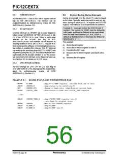
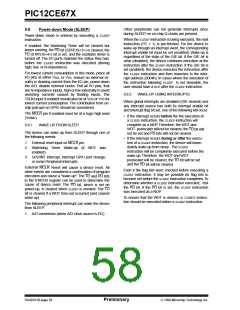
FIGURE 9-16: WATCHDOG TIMER BLOCK DIAGRAM
From TMR0 Clock Source
(Figure 7-5)
0
Postscaler
8
M
1
U
WDT Timer
X
8 - to - 1 MUX
PS2:PS0
PSA
WDT
Enable Bit
To TMR0 (Figure 7-5)
0
1
MUX
PSA
WDT
Time-out
Note: PSA and PS2:PS0 are bits in the OPTION register.
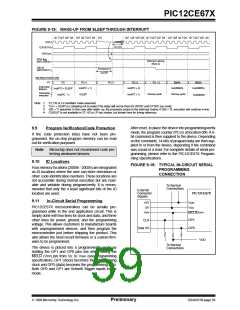
FIGURE 9-17: SUMMARY OF WATCHDOG TIMER REGISTERS
Address
2007h
81h
Name
Bit 7
MCLRE
GPPU
Bit 6
Bit 5
Bit 4
PWRTE WDTE FOSC2 FOSC1 FOSC0
T0SE PSA PS2 PS1 PS0
Bit 3
Bit 2
Bit 1
Bit 0
(1)
CP1
CP0
Config. bits
OPTION
INTEDG T0CS
Legend: Shaded cells are not used by the Watchdog Timer.
Note 1: See Figure 9-1 for operation of these bits. Not all CP0 and CP1 bits are shown.
1998 Microchip Technology Inc.
Preliminary
DS40181B-page 57

 MICROCHIP [ MICROCHIP ]