PIC12CE67X
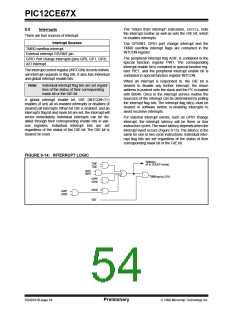
9.5.1
TMR0 INTERRUPT
9.6
Context Saving During Interrupts
During an interrupt, only the return PC value is saved
on the stack.Typically, users may wish to save key reg-
isters during an interrupt i.e., W register and STATUS
register. This will have to be implemented in software.
An overflow (FFh → 00h) in the TMR0 register will set
flag bit T0IF (INTCON<2>). The interrupt can be
enabled/disabled by setting/clearing enable bit T0IE
(INTCON<5>). (Section 7.0)
Example 9-1 store and restore the STATUS and W
registers. The register, W_TEMP, must be defined in
both banks and must be defined at the same offset
from the bank base address (i.e., if W_TEMP is
defined at 0x20 in bank 0, it must also be defined at
0xA0 in bank 1).
9.5.2
INT INTERRUPT
External interrupt on GP2/INT pin is edge triggered:
either rising if bit INTEDG (OPTION<6>) is set, or fall-
ing, if the INTEDG bit is clear. When a valid edge
appears on the GP2/INT pin, flag bit INTF
(INTCON<1>) is set. This interrupt can be disabled by
clearing enable bit INTE (INTCON<4>). Flag bit INTF
must be cleared in software in the interrupt service rou-
tine before re-enabling this interrupt. The INT interrupt
can wake-up the processor from SLEEP, if bit INTE was
set prior to going into SLEEP.The status of global inter-
rupt enable bit GIE decides whether or not the proces-
sor branches to the interrupt vector following wake-up.
See Section 9.8 for details on SLEEP mode.
The example:
a) Stores the W register.
b) Stores the STATUS register in bank 0.
c) Executes the ISR code.
d) Restores the STATUS register (and bank select
bit).
e) Restores the W register.
9.5.3
GPIO INTCON CHANGE
An input change on GP3, GP1 or GP0 sets flag bit
GPIF (INTCON<0>). The interrupt can be enabled/dis-
abled by setting/clearing enable bit GPIE
(INTCON<3>). (Section 5.1)
EXAMPLE 9-1: SAVING STATUS AND W REGISTERS IN RAM
MOVWF
SWAPF
BCF
MOVWF
:
W_TEMP
;Copy W to TEMP register, could be bank one or zero
;Swap status to be saved into W
;Change to bank zero, regardless of current bank
;Save status to bank zero STATUS_TEMP register
STATUS,W
STATUS,RP0
STATUS_TEMP
:(ISR)
:
SWAPF
STATUS_TEMP,W
;Swap STATUS_TEMP register into W
;(sets bank to original state)
;Move W into STATUS register
;Swap W_TEMP
MOVWF
SWAPF
SWAPF
STATUS
W_TEMP,F
W_TEMP,W
;Swap W_TEMP into W
DS40181B-page 56
Preliminary
1998 Microchip Technology Inc.

 MICROCHIP [ MICROCHIP ]