PIC12CE67X
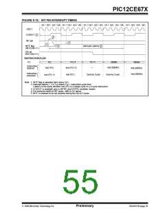
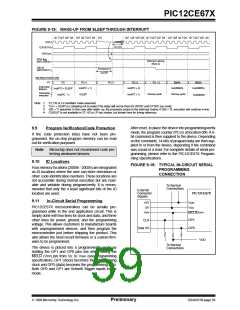
FIGURE 9-18: WAKE-UP FROM SLEEP THROUGH INTERRUPT
Q1 Q2 Q3 Q4 Q1 Q2 Q3 Q4 Q1
Q1 Q2 Q3 Q4 Q1 Q2 Q3 Q4 Q1 Q2 Q3 Q4 Q1 Q2 Q3 Q4
OSC1
TOST(2)
CLKOUT(4)
GPIO pin
GPIF flag
(INTCON<0>)
Interrupt Latency
(Note 2)
GIE bit
(INTCON<7>)
Processor in
SLEEP
INSTRUCTION FLOW
PC
PC
PC+1
PC+2
PC+2
PC + 2
0004h
0005h
Instruction
Inst(0004h)
Inst(PC + 1)
Inst(PC + 2)
Inst(0005h)
Inst(PC) = SLEEP
Inst(PC - 1)
fetched
Instruction
executed
Dummy cycle
Dummy cycle
SLEEP
Inst(PC + 1)
Inst(0004h)
Note 1: XT, HS or LP oscillator mode assumed.
2: TOST = 1024TOSC (drawing not to scale) This delay will not be there for INTRC and EXTRC osc mode.
3: GIE = '1' assumed. In this case after wake- up, the processor jumps to the interrupt routine. If GIE = '0', execution will continue in-line.
4: CLKOUT is not available in XT, HS or LP osc modes, but shown here for timing reference.
After reset, to place the device into programming/verify
mode, the program counter (PC) is at location 00h. A 6-
bit command is then supplied to the device. Depending
on the command, 14-bits of program data are then sup-
plied to or from the device, depending if the command
was a load or a read. For complete details of serial pro-
gramming, please refer to the PIC12CE67X Program-
ming Specifications.
9.9
Program Verification/Code Protection
If the code protection bit(s) have not been pro-
grammed, the on-chip program memory can be read
out for verification purposes.
Note: Microchip does not recommend code pro-
tecting windowed devices.
9.10
ID Locations
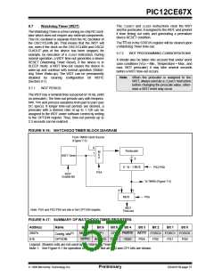
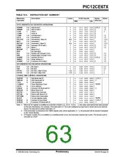
FIGURE 9-19: TYPICAL IN-CIRCUIT SERIAL
PROGRAMMING
Four memory locations (2000h - 2003h) are designated
as ID locations where the user can store checksum or
other code-identification numbers. These locations are
not accessible during normal execution but are read-
able and writable during program/verify. It is recom-
mended that only the 4 least significant bits of the ID
location are used.
CONNECTION
To Normal
Connections
External
Connector
Signals
PIC12CE67X
9.11
In-Circuit Serial Programming
+5V
0V
VDD
PIC12CE67X microcontrollers can be serially pro-
grammed while in the end application circuit. This is
simply done with two lines for clock and data, and three
other lines for power, ground, and the programming
voltage. This allows customers to manufacture boards
with unprogrammed devices, and then program the
microcontroller just before shipping the product. This
also allows the most recent firmware or a custom firm-
ware to be programmed.
VSS
VPP
MCLR/VPP
GP1
GP0
CLK
Data I/O
VDD
To Normal
Connections
The device is placed into a program/verify mode by
holding the GP1 and GP0 pins low while raising the
MCLR (VPP) pin from VIL to VIHH (see programming
specification). GP1 (clock) becomes the programming
clock and GP0 (data) becomes the programming data.
Both GP0 and GP1 are Schmitt Trigger inputs in this
mode.
1998 Microchip Technology Inc.
Preliminary
DS40181B-page 59

 MICROCHIP [ MICROCHIP ]