PIC12CE67X
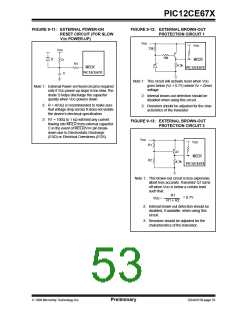
FIGURE 9-11: EXTERNAL POWER-ON
RESET CIRCUIT (FOR SLOW
VDD POWER-UP)
FIGURE 9-12: EXTERNAL BROWN-OUT
PROTECTION CIRCUIT 1
VDD
VDD
33k
VDD
10k
D
R
MCLR
R1
4.3k
MCLR
PIC12CE67X
PIC12CE67X
C
Note 1: This circuit will activate reset when VDD
goes below (Vz + 0.7V) where Vz = Zener
voltage.
Note 1: External Power-on Reset circuit is required
only if VDD power-up slope is too slow.The
diode D helps discharge the capacitor
quickly when VDD powers down.
2: Internal brown-out detection should be
disabled when using this circuit.
2: R < 40 kΩ is recommended to make sure
that voltage drop across R does not violate
the device’s electrical specification.
3: Resistors should be adjusted for the char-
acteristics of the transistor.
3: R1 = 100Ω to 1 kΩ will limit any current
flowing into MCLR from external capacitor
C in the event of MCLR/VPP pin break-
down due to Electrostatic Discharge
(ESD) or Electrical Overstress (EOS).
FIGURE 9-13: EXTERNAL BROWN-OUT
PROTECTION CIRCUIT 2
VDD
VDD
R1
Q1
MCLR
R2
4.3k
PIC12CE67X
Note 1: This brown-out circuit is less expensive,
albeit less accurate. Transistor Q1 turns
off when VDD is below a certain level
such that:
R1
= 0.7V
VDD •
R1 + R2
2: Internal brown-out detection should be
disabled, if available, when using this
circuit.
3: Resistors should be adjusted for the
characteristics of the transistor.
1998 Microchip Technology Inc.
Preliminary
DS40181B-page 53

 MICROCHIP [ MICROCHIP ]