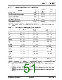
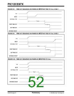
PIC12CE67X
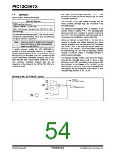
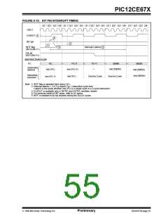
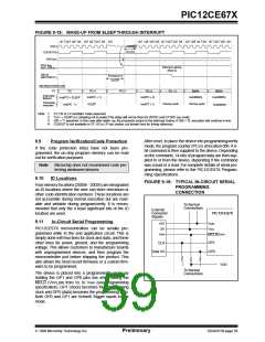
FIGURE 9-15: INT PIN INTERRUPT TIMING
Q1 Q2 Q3 Q4 Q1 Q2 Q3 Q4 Q1 Q2 Q3 Q4 Q1 Q2 Q3 Q4 Q1 Q2 Q3 Q4
OSC1
CLKOUT
3
4
INT pin
1
1
Interrupt Latency
INTF flag
(INTCON<1>)
5
2
GIE bit
(INTCON<7>)
INSTRUCTION FLOW
PC
0004h
PC+1
PC+1
—
0005h
PC
Instruction
fetched
Inst (0004h)
Inst (PC)
Inst (PC+1)
Inst (0005h)
Inst (0004h)
Instruction
executed
Dummy Cycle
Dummy Cycle
Inst (PC)
Inst (PC-1)
Note
1: INTF flag is sampled here (every Q1).
2: Interrupt latency = 3-4 Tcy where Tcy = instruction cycle time.
Latency is the same whether Inst (PC) is a single cycle or a 2-cycle instruction.
3: CLKOUT is available only in INTRC and EXTRC oscillator modes.
4: For minimum width of INT pulse, refer to AC specs.
5: INTF is enabled to be set anytime during the Q4-Q1 cycles.
1998 Microchip Technology Inc.
Preliminary
DS40181B-page 55

 MICROCHIP [ MICROCHIP ]