PIC12CE67X
The instruction set is highly orthogonal and is grouped
into three basic categories:
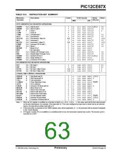
10.0 INSTRUCTION SET SUMMARY
Each PIC12CE67X instruction is a 14-bit word divided
into an OPCODE which specifies the instruction type
and one or more operands which further specify the
operation of the instruction. The PIC12CE67X instruc-
tion set summary in Table 10-2 lists byte-oriented, bit-
oriented, and literal and control operations. Table 10-
1 shows the opcode field descriptions.
• Byte-oriented operations
• Bit-oriented operations
• Literal and control operations
All instructions are executed within one single instruc-
tion cycle, unless a conditional test is true or the pro-
gram counter is changed as a result of an instruction.
In this case, the execution takes two instruction cycles
with the second cycle executed as a NOP. One instruc-
tion cycle consists of four oscillator periods. Thus, for
an oscillator frequency of 4 MHz, the normal instruction
execution time is 1 µs. If a conditional test is true or the
program counter is changed as a result of an instruc-
tion, the instruction execution time is 2 µs.
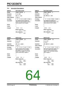
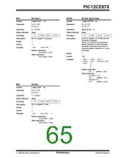
For byte-oriented instructions, 'f' represents a file reg-
ister designator and 'd' represents a destination desig-
nator. The file register designator specifies which file
register is to be used by the instruction.
The destination designator specifies where the result of
the operation is to be placed. If 'd' is zero, the result is
placed in the W register. If 'd' is one, the result is placed
in the file register specified in the instruction.
Table 10-2 lists the instructions recognized by the
MPASM assembler.
For bit-oriented instructions, 'b' represents a bit field
designator which selects the number of the bit affected
by the operation, while 'f' represents the number of the
file in which the bit is located.
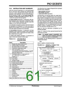
Figure 10-1 shows the three general formats that the
instructions can have.
Note: To maintain upward compatibility with
future PIC12CE67X products, do not use
the OPTIONand TRISinstructions.
For literal and control operations, 'k' represents an
eight or eleven bit constant or literal value.
All examples use the following format to represent a
hexadecimal number:
TABLE 10-1: OPCODE FIELD
DESCRIPTIONS
0xhh
Field
Description
where h signifies a hexadecimal digit.
f
W
b
k
x
Register file address (0x00 to 0x7F)
Working register (accumulator)
FIGURE 10-1: GENERAL FORMAT FOR
INSTRUCTIONS
Bit address within an 8-bit file register
Literal field, constant data or label
Byte-oriented file register operations
13
8
7
6
0
0
Don't care location (= 0 or 1)
OPCODE
d
f (FILE #)
The assembler will generate code with x = 0. It is the
recommended form of use for compatibility with all
Microchip software tools.
d = 0 for destination W
d = 1 for destination f
f = 7-bit file register address
d
Destination select; d = 0: store result in W,
d = 1: store result in file register f.
Default is d = 1
Bit-oriented file register operations
13 10 9
7 6
label Label name
TOS Top of Stack
PC Program Counter
OPCODE
b (BIT #)
f (FILE #)
b = 3-bit bit address
f = 7-bit file register address
PCLATH
Program Counter High Latch
GIE Global Interrupt Enable bit
WDT Watchdog Timer/Counter
TO Time-out bit
Literal and control operations
General
13
8
7
0
0
OPCODE
k (literal)
PD Power-down bit
dest Destination either the W register or the specified
k = 8-bit immediate value
CALLand GOTOinstructions only
13 11 10
OPCODE
k = 11-bit immediate value
register file location
[ ] Options
Contents
( )
→
k (literal)
Assigned to
Register bit field
In the set of
< >
User defined term (font is courier)
italics
1998 Microchip Technology Inc.
Preliminary
DS40181B-page 61

 MICROCHIP [ MICROCHIP ]