KSZ8795CLX
3.5.1.2
MII Management Interface (MIIM)
The KSZ8795CLX supports the standard IEEE 802.3 MII management interface, also known as the management data
input/output (MDIO) interface. This interface allows upper-layer devices to monitor and control the states of the
KSZ8795CLX. An external device with MDC/MDIO capability is used to read the PHY status or configure the PHY set-
tings. Further details on the MIIM interface are found in the IEEE 802.3u Specification.
The MIIM interface consists of the following:
• A physical connection that incorporates the data line MDIO and the clock line MDC.
• A specific protocol that operates across the aforementioned physical connection that allows an external controller
to communicate with the KSZ8795CLX device.
• Access to a set of eight 16-bit registers, consisting of 8 standard MIIM Registers [0:5h], 1d and 1f MIIM registers
per port.
The MIIM interface MDC/MDIO can operate up to a maximum clock speed of 25 MHz MDC clock.
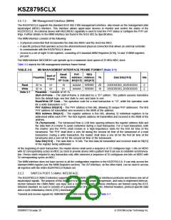
Table 3-6 depicts the MII management interface frame format.
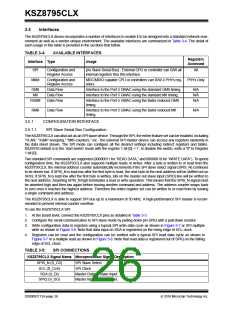
TABLE 3-6:
MII MANAGEMENT INTERFACE FRAME FORMAT (Note 3-1)
Read/
Write
PHY
REG
Start of
Frame
Preamble
Address Address
TA
Data Bits[15:0]
Idle
OP Code Bits[4:0] Bits[4:0]
Read
32 1s
32 1s
01
01
10
01
AAAAA
AAAAA
RRRRR
RRRRR
Z0
10
DDDDDDDD_DDDDDDDD
DDDDDDDD_DDDDDDDD
Z
Z
Write
Note 3-1
Preamble – Consists of 32 1s
Start-of-Frame – The start-of-frame is indicated by a “01” pattern. This pattern assures transitions
from the default logic one line state to zero and back to one.
Read/Write OP Code – The operation code for a read transaction is “10”, while the operation code
for a write transaction is 01.
PHY Address Bits[4:0] – The PHY address is five bits, allowing 32 unique PHY addresses. The first
PHY address bit transmitted and received is the MSB of the address.
REG Address Bits[4:0] – The register address is five bits, allowing 32 individual registers to be
addressed within each PHY. The first register address bit transmitted and received is the MSB of the
address.
TA (Turnaround) – The turnaround time is 2-bit time spacing between the register address field and
the data field of a frame to avoid contention during a read transaction. For a read transaction, both
the master and the PHYs shall remain in a high-impedance state for the first bit time of the
turnaround. The PHY shall drive a zero bit during the second bit time of the turnaround of a read
transaction. During a write transaction, the master shall drive a one bit for the first bit time of the
turnaround and a zero bit for the second bit time of the turnaround.
Data Bits[15:0] – The data field is 16 bits. The first data bit transmitted and received shall be Bit[15]
of the register being addressed.
At the beginning of each transaction, the master device shall send a sequence of 32 contiguous logic 1 bits on MDIO
with 32 corresponding cycles on MDC as clock to provide device with a pattern that it can use to establish synchroniza-
tion. Device starts respond to any transaction only after observes a sequence of 32 contiguous one bits on MDIO with
32 corresponding cycles on MDC.
The MIIM interface does not have access to all the configuration registers in the KSZ8795CLX. It can only access the
standard MIIM register (see the MIIM Registers section). The SPI interface, on the other hand, can be used to access
all registers with the entire KSZ8795CLX feature set.
3.5.2
SWITCH PORT 5 GMAC INTERFACE
The KSZ8795CLX GMAC5 interface supports the GMII/MII/RGMII/RMII four interfaces protocols and shares one set of
input/output signals. The purpose of this interface is to provide a simple, inexpensive, and easy-to implement intercon-
nection between the GMAC/MAC sub layer and a GPHY/PHY. Data on these interfaces are framed using the IEEE
Ethernet standard. As such it consists of a preamble, start of frame delimiter, Ethernet headers, protocol-specific data
and a cyclic redundancy check (CRC) checksum.
Transmit and receive signals for GMII/MII/RGMII/RMII interfaces shown in Table 3-7.
DS00002112A-page 28
2016 Microchip Technology Inc.

 MICREL [ MICREL SEMICONDUCTOR ]