KSZ8795CLX
3.5
Interfaces
The KSZ8795CLX device incorporates a number of interfaces to enable it to be designed into a standard network envi-
ronment as well as a vendor unique environment. The available interfaces are summarized in Table 3-4. The detail of
each usage in this table is provided in the sections that follow.
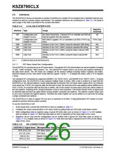
TABLE 3-4:
AVAILABLE INTERFACES
Registers
Accessed
Interface Type
Usage
SPI
Configuration and
Register Access
[As Slave Serial Bus] - External CPU or controller can R/W all
internal registers thru this interface.
All
MIIM
Configuration and
Register Access
MDC/MDIO capable CPU or controllers can R/W 4 PHYs reg-
isters.
PHYs Only
GMII
MII
Data Flow
Data Flow
Data Flow
Interface to the Port 5 GMAC using the standard GMII timing.
Interface to the Port 5 GMAC using the standard MII timing.
N/A
N/A
N/A
RGMII
Interface to the Port 5 GMAC using the faster reduced GMII
timing.
RMII
Data Flow
Interface to the Port 5 GMAC using the faster reduced MII
timing.
N/A
3.5.1
3.5.1.1
CONFIGURATION INTERFACE
SPI Slave Serial Bus Configuration
The KSZ8795CLX can also act as an SPI slave device. Through the SPI, the entire feature set can be enabled, including
“VLAN,” “IGMP snooping,” “MIB counters,” etc. The external SPI master device can access any registers randomly in
the data sheet shown. The SPI mode can configure all the desired settings including indirect registers and tables.
KSZ8795 default is in the ‘start switch’ mode with the register 1 bit [0] =’1’, to disable the switch, write a "0" to Register
1 bit [0].
Two standard SPI commands are supported (00000011 for “READ DATA,” and 00000010 for “WRITE DATA”). To speed
configuration time, the KSZ8795CLX also supports multiple reads or writes. After a byte is written to or read from the
KSZ8795CLX, the internal address counter automatically increments if the SPI slave select signal (SPIS_N) continues
to be driven low. If SPIS_N is kept low after the first byte is read, the next byte at the next address will be shifted out on
SPIQ. If SPIS_N is kept low after the first byte is written, bits on the master out slave input (SPID) line will be written to
the next address. Asserting SPIS_N high terminates a read or write operation. This means that the SPIS_N signal must
be asserted high and then low again before issuing another command and address. The address counter wraps back
to zero once it reaches the highest address. Therefore the entire register set can be written to or read from by issuing
a single command and address.
The KSZ8795CLX is able to support SPI bus up to a maximum of 50 MHz. A high-performance SPI master is recom-
mended to prevent internal counter overflow.
To use the KSZ8795CLX SPI:
1. At the board level, connect the KSZ8795CLX pins as detailed in Table 3-5.
2. Configure the serial communication to SPI slave mode by pulling down pin SPIQ with a pull-down resistor.
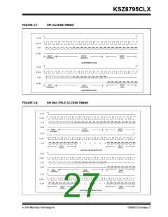
3. Write configuration data to registers using a typical SPI write data cycle as shown in Figure 3-7 or SPI multiple
write as shown in Figure 3-8. Note that data input on SDA is registered on the rising edge of SCL clock.
4. Registers can be read and the configuration can be verified with a typical SPI read data cycle as shown in
Figure 3-7 or a multiple read as shown in Figure 3-8. Note that read data is registered out of SPIQ on the falling
edge of SCL clock.
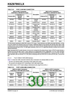
TABLE 3-5:
SPI CONNECTIONS
KSZ8795CLX Signal Name Microprocessor Signal Description
SPIS_N (S_CS)
SCL (S_CLK)
SDA (S_DI)
SPI Slave Select
SPI Clock
Master Output. Slave Input.
Master Input. Slave Output.
SPIQ (S_DO)
DS00002112A-page 26
2016 Microchip Technology Inc.

 MICREL [ MICREL SEMICONDUCTOR ]