KSZ8795CLX
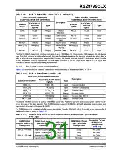
TABLE 3-9:
PORT 5 SW5-GMII CONNECTION (CONTINUED)
GMAC-to-GMAC Connection
GMAC-to-GPHY Connection
KSZ8795CLX SW5-GMII GPHY Mode
KSZ8795CLX SW5-GMII GMAC Mode
Description
KSZ8795CLX
External
GMAC
KSZ8795CLX
External
GPHY
SW5-GMII
Signals
Type
SW5-GMII
Signals
Type
MCOL
COL5
Output
Collision
MCOL
COL5
Input
Detection
MCRS
CRS5
Output
Output
Carrier Sense
MCRS
CRS5
Input
Input
MRXEN
RXDV5
Receive Data
Valid
MRXDV
TXEN5
MTXER
RXER5
Output
Output
Receive Error
MRXER
TXER5
Input
Input
MRXD[7:0]
RXD5[7:0]
Receive Data
Bits[7:0]
MRXD[7:0]
TXD5[7:0]
MGTXC
GRXC5
Output
Receive Clock
MGRXC
GTXC5
Input
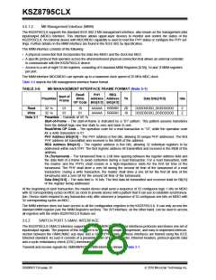
The Port 5 GMAC5 SW5-GMII interface operates at up to 1000 Mbps. In 1Gbps mode, GMII supports the full-duplex
only. The GMII interface is 8-bits data in each direction. Additional signals on the transmit side indicate when data is
valid or when an error occurs during transmission. Likewise, the receive side has indicators that convey when the data
is valid and without physical layer errors. For half-duplex operation in 10/100 Mbps mode, there is a COL signal that
indicates a collision has occurred during transmission.
3.5.2.6
Port 5 GMAC5 SW5-RGMII Interface
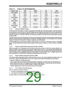
Table 3-10 shows the RGMII reduced connections when connecting to an external GMAC or GPHY.
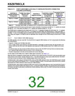
TABLE 3-10: PORT 5 SW5-RGMII CONNECTION
KSZ8795CLX SW5-RGMII Connection
Description
KSZ8795CLX SW5-RGMII
External GMAC/GPHY
Type
Signals
MRX_CTL
MRXD[3:0]
MRX_CLK
MTX_CLK
MTXD[3:0]
MGTX_CLK
TXD5_CTL
TXD5[3:0]
GTX5_CLK
RXD5_CTL
RXD5[3:0]
GRXC5
Input
Input
Transmit Control
Transmit Data Bit[3:0]
Transmit Clock
Input
Output
Output
Output
Receive Control
Receive Data Bit[3:0]
Receive Clock
The RGMII interface operates at up to a 1000 Mbps speed rate. Additional transmit and receive signals control the dif-
ferent direction of the data transfer. This RGMII interface supports RGMII Rev 2.0 with adjustable ingress clock and
egress clock delay by the Register 86 (0x56).
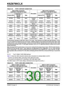
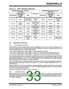
For RGMII to correctly configure with the connection partner, Register 86 (0x56) bits [4:3] need to be set up correctly. A
configuration table is found in Table 3-11.
TABLE 3-11: PORT 5 SW5-RGMII CLOCK DELAY CONFIGURATION WITH CONNECTION
PARTNER
Connection Partner
KSZ8795CLX
Register 86 Bits[4:3]
Configuration
RGMII Clock Mode
(Receive and
Transmit)
KSZ8795CLX RGMII
Clock Delay/Slew
Configuration
KSZ8795CLX
Register 86 (0x56)
RGMII Clock
Configuration
(Note 3-1)
Bit[4:3] = 11 Mode
Bit[4:3] = 10 Mode
Ingress Clock Input
Egress Clock Output
Ingress Clock Input
Egress Clock Output
Bit[4] = 1
Bit[3] = 1
Bit[4] = 1
Bit[3] = 1
Delay
Delay
No Delay
No Delay
No Delay
Delay
Delay
No Delay
2016 Microchip Technology Inc.
DS00002112A-page 31

 MICREL [ MICREL SEMICONDUCTOR ]