KSZ8795CLX
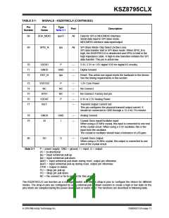
TABLE 2-1:
SIGNALS - KSZ8795CLX (CONTINUED)
Pin
Number
Pin
Name
Type
Note 2-1
Port
Description
68
69
SDA_MDIO
SPIS_N
Ipu/O
Ipu
All
Data for SPI or MDC/MDIO Interface:
Serial data input in SPI slave mode.
MDC/MDIO interface data input/output.
All
SPI Slave Mode Chip Select (Active-Low):
SPI data transfer start in SPI slave mode. When SPIS_N is
high, the KSZ8795CLX is deselected and SPIQ is held in the
high impedance state. A high-to-low transition initiates the SPI
data transfer. This pin is active-low.
70
71
72
VDDIO
GNDD
RST_N
P
—
—
—
3.3V, 2.5V or 1.8V digital VDD for digital I/O circuitry.
Digital Ground.
GND
Ipu
Reset: This active-low signal resets the hardware in the device.
See the timing requirements in this section.
73
74
75
76
77
VDD12D
NC
P
NC
NC
P
—
—
—
—
—
1.2V Core Power.
No Connect.
ATST
VDDAT
ISET
No Connect. Factory test pin.
3.3V or 2.5V Analog Power.
Transmit Output Current Set:
This pin configures the physical transmit output current. It
should be connected to GND through a 12.4 kΩ 1% resistor.
78
79
GNDA
XI
GND
I
—
—
Analog Ground.
Crystal Clock Input/Oscillator Input:
When using a 25 MHz crystal, this input is connected to one end
of the crystal circuit. When using a 3.3V oscillator, this is the
input from the oscillator.
The crystal or oscillator should have a tolerance of ±50 ppm.
80
XO
O
—
Crystal Clock Output:
When using a 25 MHz crystal, this output is connected to one
end of the crystal circuit.
Note 2-1
P = power supply; GND = ground; I = input; O = output
I/O = bi-directional
Ipu = Input w/internal pull-up.
Ipd = Input w/internal pull-down.
Ipd/O = Input w/internal pull-down during reset, output pin otherwise.
Ipu/O = Input w/internal pull-up during reset, output pin otherwise.
OTRI = Output tri-stated.
PU = Strap pin pull-up.
PD = Strap pin pull-down.
NC = No connect or tie-to-ground for this product.
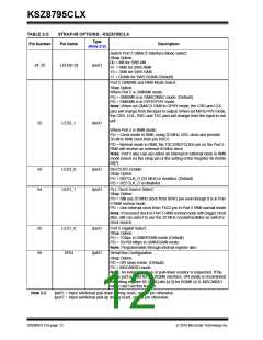
The KSZ8795CLX can function as a managed switch and utilizes strap-in pins to configure the device for different
modes. The strap-in pins are configured by using external pull-up/down resistors to create a high or low state on the
pins which are sampled during the power-down reset or warm reset. The functions are described in following table.
2016 Microchip Technology Inc.
DS00002112A-page 11

 MICREL [ MICREL SEMICONDUCTOR ]