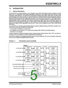
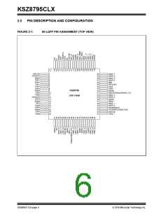
KSZ8795CLX
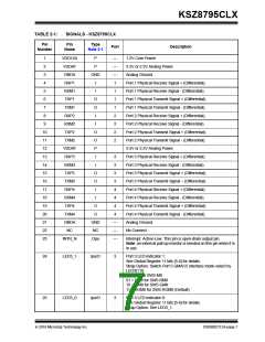
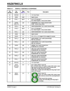
TABLE 2-1:
SIGNALS - KSZ8795CLX
Pin
Number
Pin
Name
Type
Note 2-1
Port
Description
1
2
VDD12A
VDDAT
GNDA
RXP1
RXM1
TXP1
P
—
—
—
1
1.2V Core Power
P
3.3V or 2.5V Analog Power.
Analog Ground.
3
GND
4
I
Port 1 Physical Receive Signal + (Differential).
Port 1 Physical Receive Signal - (Differential).
Port 1 Physical Transmit Signal + (Differential).
Port 1 Physical Transmit Signal - (Differential).
Port 2 Physical Receive Signal + (Differential).
Port 2 Physical Receive Signal - (Differential).
Port 2 Physical Transmit Signal + (Differential).
Port 2 Physical Transmit Signal - (Differential).
3.3V or 2.5V Analog Power.
5
I
1
6
O
1
7
TXM1
RXP2
RXM2
TXP2
O
1
8
I
2
9
I
O
2
10
11
12
13
14
15
16
17
18
19
20
21
22
23
2
TXM2
VDDAT
RXP3
RXM3
TXP3
O
2
P
I
3
3
Port 3 Physical Receive Signal + (Differential).
Port 3 Physical Receive Signal - (Differential).
Port 3 Physical Transmit Signal + (Differential).
Port 3 Physical Transmit Signal – (Differential).
Port 4 Physical Receive Signal + (Differential).
Port 4 Physical Receive Signal - (Differential).
Port 4 Physical Transmit Signal + (Differential).
Port 4 Physical Transmit Signal - (Differential).
Analog Ground.
I
O
3
TXM3
RXP4
RXM4
TXP4
O
3
I
4
I
4
O
4
TXM4
GNDA
NC
O
4
GND
NC
Opu
—
—
—
No Connect.
INTR_N
Interrupt: Active-Low. This pin is open-drain output pin.
Note: an external pull-up resistor is needed on this pin when it is
in use.
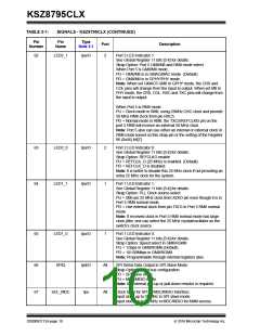
24
LED3_1
Ipu/O
3
Port 3 LED Indicator 1:
See Global Register 11 bits [5:4] for details.
Strap Option: Switch Port 5 GMAC5 interface mode select by
LED3[1:0]
00 = MII for SW5-MII
01 = RMII for SW5-RMII
10 = GMII for SW5-GMII
11 = RGMII for SW5-RGMII (Default)
25
LED3_0
Ipu/O
3
Port 3 LED Indicator 0:
See Global Register 11 bits [5:4] for details.
Strap Option: See LED3_1.
2016 Microchip Technology Inc.
DS00002112A-page 7

 MICREL [ MICREL SEMICONDUCTOR ]