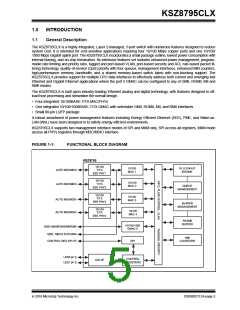
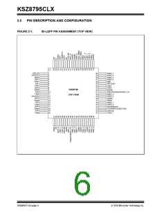
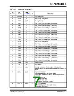
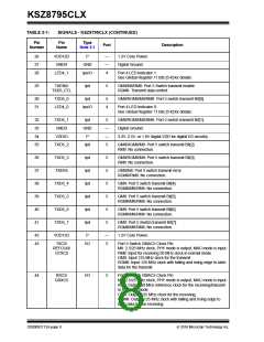
KSZ8795CLX
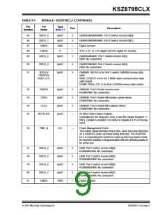
TABLE 2-1:
SIGNALS - KSZ8795CLX (CONTINUED)
Pin
Number
Pin
Name
Type
Note 2-1
Port
Description
45
46
47
48
49
RXD5_0
RXD5_1
GNDD
Ipd/O
Ipd/O
GND
P
5
5
GMII/RGMII/MII/RMII: Port 5 Switch receive Bit[0].
GMII/RGMII/MII/RMII: Port 5 Switch receive Bit[1].
Digital Ground.
—
—
5
VDDIO
3.3V, 2.5V, or 1.8V digital VDD for digital I/O circuitry.
RXD5_2
Ipd/O
GMII/RGMII/MII: Port 5 Switch receive Bit[2].
RMII: No connection
50
51
RXD5_3
Ipd/O
Ipd/O
5
5
GMII/RGMII/MII: Port 5 Switch receive Bit[3].
RMII: No connection
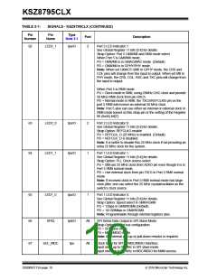
RXDV5/
CRSDV5/
RXD5_CTL
GMII/MII: RXDV5 is for Port 5 switch GMII/MII receive data
valid.
RMII: CRSDV5 is for Port 5 RMII carrier sense/receive data
valid output.
RGMII: RXD5_CTL is for Port 5 RGMII receive data control
52
53
54
55
RXER5
CRS5
Ipd/O
Ipd/O
Ipd/O
Ipu/O
5
5
GMII/MII: Port 5 Switch receive error.
RGMII/RMII: No connection.
GMII/MII: Port 5 Switch MII modes carrier sense.
RGMII/RMII: No connection.
COL5
5
GMII/MII: Port 5 Switch MII collision detect.
RGMII/RMII: No connection.
REFCLKO
—
25 MHz Clock Output (Option)
Controlled by the strap pin LED2_0 and the Global Register 11
Bit[1]. Default is enabled; it is better to disable it if it’s not being
used.
56
PME_N
I/O
—
Power Management Event
This output signal indicates that a WoL event has been detected
as a result of a wake-up frame being detected. The KSZ8795-
CLX is requesting the system to wake up from low power mode.
Its assertion polarity is programmable with the default polarity to
be active-low.
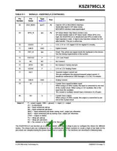
57
58
59
60
61
RXD5_4
RXD5_5
RXD5_6
RXD5_7
GNDD
Ipd/O
Ipd/O
Ipd/O
Ipd/O
GND
5
5
GMII: Port 5 switch receive Bit[4].
RGMII/MI/RMII: No connection.
GMII: Port 5 switch receive Bit[5].
RGMII/MII/RMII: No connection.
5
GMII: Port 5 switch receive Bit[6].
RGMII/MII/RMII: No connection.
5
GMII: Port 5 switch receive Bit[7].
RGMII/MII/RMII: No connection.
—
Digital Ground.
2016 Microchip Technology Inc.
DS00002112A-page 9

 MICREL [ MICREL SEMICONDUCTOR ]