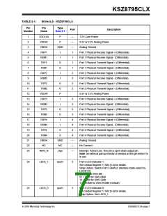
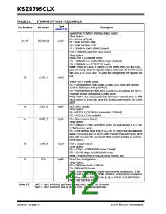
KSZ8795CLX
TABLE 2-1:
SIGNALS - KSZ8795CLX (CONTINUED)
Pin
Number
Pin
Name
Type
Note 2-1
Port
Description
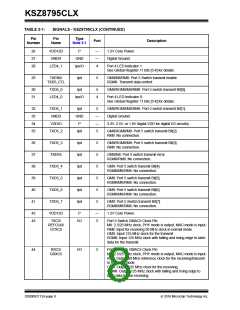
26
27
28
VDD12D
GNDD
P
—
—
4
1.2V Core Power.
Digital Ground.
GND
Ipu/O
LED4_1
Port 4 LED Indicator 1:
See Global Register 11 bits [5:4] for details.
29
TXEN5/
TXD5_CTL
Ipd
5
GMII/MII/RMII: Port 5 Switch transmit enable.
RGMII: Transmit data control.
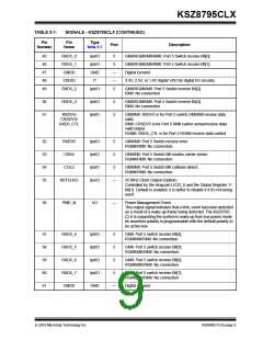
30
31
TXD5_0
LED4_0
Ipd
5
4
GMII/RGMII/MII/RMII: Port 5 switch transmit Bit[0].
Ipu/O
Port 4 LED Indicator 0:
See Global Register 11 bits [5:4] for details.
32
33
34
35
TXD5_1
GNDD
Ipd
GND
P
5
—
—
5
GMII/RGMII/MII/RMII: Port 5 switch transmit Bit[1].
Digital Ground.
VDDIO
TXD5_2
3.3V, 2.5V, or 1.8V digital VDD for digital I/O circuitry.
Ipd
GMII/RGMII/MII: Port 5 switch transmit Bit[2].
RMII: No connection.
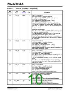
36
37
38
39
40
41
TXD5_3
TXER5
Ipd
Ipd
Ipd
Ipd
Ipd
Ipd
5
5
5
5
5
5
GMII/RGMII/MII: Port 5 switch transmit Bit[3].
RMII: No connection.
GMII/MII: Port 5 switch transmit error.
RGMII/RMII: No connection.
TXD5_4
TXD5_5
TXD5_6
TXD5_7
VDD12D
GMII: Port 5 switch transmit Bit[4].
RGMII/MII/RMII: No connection.
GMII: Port 5 switch transmit Bit[5].
RGMII/MII/RMII: No connection.
GMII: Port 5 switch transmit Bit[6].
RGMII/MII/RMII: No connection.
GMII: Port 5 Switch transmit Bit[7].
RGMII/MII/RMII: No connection.
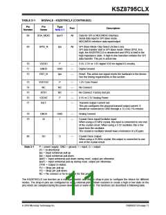
42
43
P
—
5
1.2V Core Power.
TXC5/
REFCLKI/
GTXC5
I/O
Port 5 Switch GMAC5 Clock Pin:
MII: 2.5/25 MHz clock, PHY mode is output, MAC mode is input.
RMII: Input for receiving 50 MHz clock in normal mode
GMII: Input 125 MHz clock for the transmit
RGMII: Input 125 MHz clock with falling and rising edge to latch
data for the transmit.
44
RXC5/
I/O
5
Port 5 Switch GMAC5 Clock Pin:
GRXC5
MII: 2.5/25 MHz clock, PHY mode is output, MAC mode is input.
RMII: Output 50 MHz reference clock for the receiving/transmit
in the clock mode.
GMII: Output 125 MHz clock for the receiving.
RGMII: Output 125 MHz clock with falling and rising edge to
latch data for the receiving.
DS00002112A-page 8
2016 Microchip Technology Inc.

 MICREL [ MICREL SEMICONDUCTOR ]