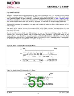
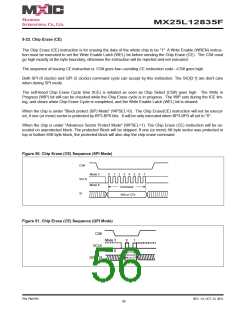
MX25L12835F
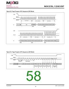
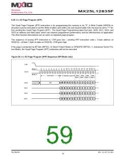
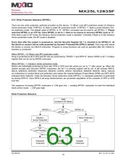
9-25. 4 x I/O Page Program (4PP)
The Quad Page Program (4PP) instruction is for programming the memory to be "0". A Write Enable (WREN) in-
struction must be executed to set the Write Enable Latch (WEL) bit and Quad Enable (QE) bit must be set to "1" be-
fore sending the Quad Page Program (4PP). The Quad Page Programming takes four pins: SIO0, SIO1, SIO2, and
SIO3 as address and data input, which can improve programmer performance and the effectiveness of application.
The other function descriptions are as same as standard page program.
The sequence of issuing 4PP instruction is: CS# goes low→ sending 4PP instruction code→ 3-byte address on
SIO[3:0]→ at least 1-byte on data on SIO[3:0]→CS# goes high.
If the page is protected by BP bits (WPSEL=0; Block Protect Mode) or SPB/DPB (WPSEL=1; Advanced Sector Pro-
tect Mode), the Quad Page Program (4PP) instruction will not be executed.
Figure 54. 4 x I/O Page Program (4PP) Sequence (SPI Mode only)
CS#
10 11 12 13 14 15 16 17 18 19 20 21
Data Data Data Data
0
1
2
3
4
5
6
7
8
9
Mode 3
Mode 0
SCLK
Command
38h
6 Address cycle
Byte 1 Byte 2 Byte 3 Byte 4
A16
A8 A4 A0
A12
A20
4
0
4
0
4
0
4
0
SIO0
SIO1
SIO2
SIO3
A21 A17 A13 A9 A5 A1
5
6
7
1
2
3
5
6
7
1
2
3
5
6
7
1
2
3
5
6
7
1
2
3
A22
A14 A10 A6 A2
A18
A7
A23 A19 A15 A11
A3
P/N: PM1795
REV. 1.0, OCT. 23, 2012
59

 Macronix [ MACRONIX INTERNATIONAL ]