MX25L12835F
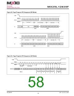
9-24. Page Program (PP)
The Page Program (PP) instruction is for programming the memory to be "0". A Write Enable (WREN) instruction
must be executed to set the Write Enable Latch (WEL) bit before sending the Page Program (PP). The device pro-
grams only the last 256 data bytes sent to the device. If the entire 256 data bytes are going to be programmed, A7-
A0 (The eight least significant address bits) should be set to 0. If the eight least significant address bits (A7-A0) are
not all 0, all transmitted data going beyond the end of the current page are programmed from the start address of
the same page (from the address A7-A0 are all 0). If more than 256 bytes are sent to the device, the data of the
last 256-byte is programmed at the requested page and previous data will be disregarded. If less than 256 bytes
are sent to the device, the data is programmed at the requested address of the page without effect on other address
of the same page.
The sequence of issuing PP instruction is: CS# goes low→ sending PP instruction code→ 3-byte address on SI→ at
least 1-byte on data on SI→ CS# goes high.
The CS# must be kept to low during the whole Page Program cycle; The CS# must go high exactly at the byte
boundary( the latest eighth bit of data being latched in), otherwise the instruction will be rejected and will not be ex-
ecuted.
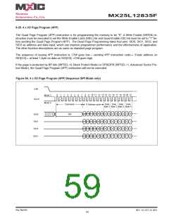
The self-timed Page Program Cycle time (tPP) is initiated as soon as Chip Select (CS#) goes high. The Write in
Progress (WIP) bit still can be checked while the Page Program cycle is in progress. The WIP sets during the tPP
timing, and clears when Page Program Cycle is completed, and the Write Enable Latch (WEL) bit is cleared. If the
Block is protected by BP bits (WPSEL=0; Block Protect Mode) or SPB/DPB (WPSEL=1; Advanced Sector Protect
Mode) the Page Program (PP) instruction will not be executed.
Both SPI (8 clocks) and QPI (2 clocks) command cycle can accept by this instruction. The SIO[3:1] are don't care
when during SPI mode.
P/N: PM1795
REV. 1.0, OCT. 23, 2012
57

 Macronix [ MACRONIX INTERNATIONAL ]