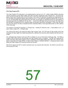
MX25L12835F
9-27. Enter Secured OTP (ENSO)
The ENSO instruction is for entering the additional 4K-bit secured OTP mode. While device is in 4K-bit secured
OTPmode, main array access is not available. The additional 4K-bit secured OTP is independent from main array
and may be used to store unique serial number for system identifier. After entering the Secured OTP mode, follow
standard read or program procedure to read out the data or update data. The Secured OTP data cannot be updated
again once it is lock-down.
The sequence of issuing ENSO instruction is: CS# goes low→ sending ENSO instruction to enter Secured OTP
mode→ CS# goes high.
Both SPI (8 clocks) and QPI (2 clocks) command cycle can accept by this instruction. The SIO[3:1] are don't care
when during SPI mode.
Please note that after issuing ENSO command user can only access secure OTP region with standard read or pro-
gram procedure. Furthermore, once security OTP is lock down, only read related commands are valid.
9-28. Exit Secured OTP (EXSO)
The EXSO instruction is for exiting the additional 4K-bit secured OTP mode.
The sequence of issuing EXSO instruction is: CS# goes low→ sending EXSO instruction to exit Secured OTP
mode→ CS# goes high.
Both SPI (8 clocks) and QPI (2 clocks) command cycle can accept by this instruction. The SIO[3:1] are don't care
when during SPI mode.
9-29. Read Security Register (RDSCUR)
The RDSCUR instruction is for reading the value of Security Register bits. The Read Security Register can be read
at any time (even in program/erase/write status register/write security register condition) and continuously.
The sequence of issuing RDSCUR instruction is : CS# goes low→sending RDSCUR instruction→Security Register
data out on SO→ CS# goes high.
Both SPI (8 clocks) and QPI (2 clocks) command cycle can accept by this instruction. The SIO[3:1] are don't care
when during SPI mode.
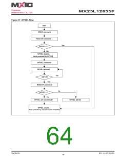
9-30. Write Security Register (WRSCUR)
The WRSCUR instruction is for changing the values of Security Register Bits. The WREN (Write Enable) instruction
is required before issuing WRSCUR instruction. The WRSCUR instruction may change the values of bit1 (LDSO
bit) for customer to lock-down the 4K-bit Secured OTP area. Once the LDSO bit is set to "1", the Secured OTP area
cannot be updated any more.
The sequence of issuing WRSCUR instruction is :CS# goes low→ sending WRSCUR instruction → CS# goes high.
Both SPI (8 clocks) and QPI (2 clocks) command cycle can accept by this instruction. The SIO[3:1] are don't care
when during SPI mode.
The CS# must go high exactly at the boundary; otherwise, the instruction will be rejected and not executed.
P/N: PM1795
REV. 1.0, OCT. 23, 2012
61

 Macronix [ MACRONIX INTERNATIONAL ]