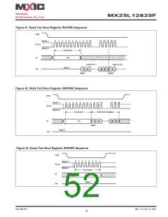
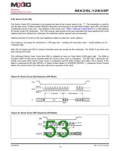
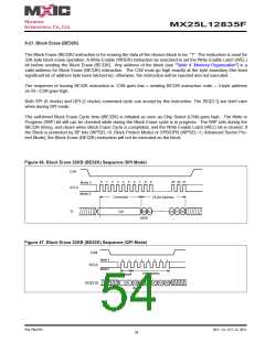
MX25L12835F
9-23. Chip Erase (CE)
The Chip Erase (CE) instruction is for erasing the data of the whole chip to be "1". A Write Enable (WREN) instruc-
tion must be executed to set the Write Enable Latch (WEL) bit before sending the Chip Erase (CE). The CS# must
go high exactly at the byte boundary, otherwise the instruction will be rejected and not executed.
The sequence of issuing CE instruction is: CS# goes low→sending CE instruction code→CS# goes high.
Both SPI (8 clocks) and QPI (2 clocks) command cycle can accept by this instruction. The SIO[3:1] are don't care
when during SPI mode.
The self-timed Chip Erase Cycle time (tCE) is initiated as soon as Chip Select (CS#) goes high. The Write in
Progress (WIP) bit still can be checked while the Chip Erase cycle is in progress. The WIP sets during the tCE tim-
ing, and clears when Chip Erase Cycle is completed, and the Write Enable Latch (WEL) bit is cleared.
When the chip is under "Block protect (BP) Mode" (WPSEL=0). The Chip Erase(CE) instruction will not be execut-
ed, if one (or more) sector is protected by BP3-BP0 bits. It will be only executed when BP3-BP0 all set to "0".
When the chip is under "Advances Sector Protect Mode" (WPSEL=1). The Chip Erase (CE) instruction will be ex-
ecuted on unprotected block. The protected Block will be skipped. If one (or more) 4K byte sector was protected in
top or bottom 64K byte block, the protected block will also skip the chip erase command.
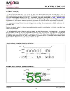
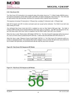
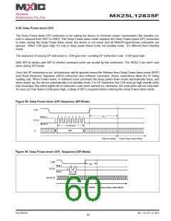
Figure 50. Chip Erase (CE) Sequence (SPI Mode)
CS#
Mode 3
Mode 0
0
1
2
3
4
5
6
7
SCLK
SI
Command
60h or C7h
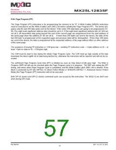
Figure 51. Chip Erase (CE) Sequence (QPI Mode)
CS#
0
1
Mode 3
Mode 0
SCLK
Command
60h or C7h
SIO[3:0]
P/N: PM1795
REV. 1.0, OCT. 23, 2012
56

 Macronix [ MACRONIX INTERNATIONAL ]