5V, Differential Input, DirectDrive, 130mW
Stereo Headphone Amplifiers with Shutdown
Shutdown
The MAX9722A/MAX9722B feature shutdown control
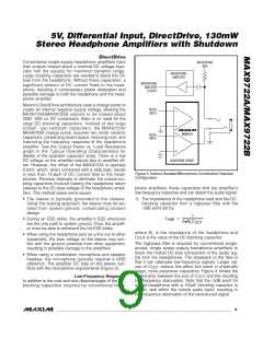
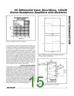
OUTPUT POWER vs. SUPPLY VOLTAGE
allowing audio signals to be shut down or muted.
160
Driving SHDN low disables the amplifiers and the
f
= 1kHz
IN
L
INPUTS 180°
OUT OF PHASE
R = 32Ω
THD+N = 10%
charge pump, sets the amplifier output impedance to
10kΩ, and reduces the supply current. In shutdown
mode, the supply current is reduced to 0.1µA. The
charge pump is enabled once SHDN is driven high.
140
120
100
80
Applications Information
60
INPUTS
IN PHASE
Power Dissipation
Under normal operating conditions, linear power ampli-
fiers can dissipate a significant amount of power. The
maximum power dissipation for each package is given
in the Absolute Maximum Ratings section under
Continuous Power Dissipation or can be calculated by
the following equation:
40
20
0
2.4 2.6 2.8 3.0 3.2 3.4 3.6 3.8 4.0
SUPPLY VOLTAGE (V)
T
- T
A
Figure 6. Output Power vs. Supply Voltage With Inputs In/Out
of Phase
J(MAX)
P
=
DISSPKG(MAX)
θ
JA
imum attainable output power. Figure 6 shows the two
extreme cases for in- and out-of-phase. In reality, the
available power lies between these extremes.
where T
is +145°C, T is the ambient tempera-
A
J(MAX)
ture, and θ is the reciprocal of the derating factor in
JA
°C/W as specified in the Absolute Maximum Ratings
section. For example, θ of the thin QFN package is
JA
Powering Other Circuits
from a Negative Supply
+63.8°C/W, and 99.3°C/W for the TSSOP package.
The MAX9722A/MAX9722B have two power dissipation
sources: the charge pump and two amplifiers. If power
dissipation for a given application exceeds the maxi-
mum allowed for a particular package, either reduce
An additional benefit of the MAX9722A/MAX9722B is
the internally generated, negative supply voltage
(PV ). This voltage provides the ground-referenced
SS
output level. PV
can, however, be used to power
SS
SV , increase load impedance, decrease the ambient
DD
other devices within a design limit current drawn from
PV to 5mA; exceeding this affects the headphone
temperature, or add heatsinking to the device. Large
output, supply, and ground traces improve the maxi-
mum power dissipation in the package.
SS
amplifier operation. A typical application is a negative
supply to adjust the contrast of LCD modules.
Thermal-overload protection limits total power dissipa-
tion in the MAX9722A/MAX9722B. When the junction
temperature exceeds +145°C, the thermal-protection
circuitry disables the amplifier output stage. The ampli-
fiers are enabled once the junction temperature cools
by 5°C. This results in a pulsing output under continu-
ous thermal-overload conditions.
PV is roughly proportional to PV and is not a regulat-
SS
DD
ed voltage. The charge-pump output impedance must be
taken into account when powering other devices from
PV . The charge-pump output impedance plot appears
SS
in the Typical Operating Characteristics. For best results,
use 1µF charge-pump capacitors.
UVLO
The MAX9722A/MAX9722B feature an UVLO function
that prevents the device from operating if the supply
voltage is less than 2.2V (typ). This feature ensures
proper operation during brownout conditions and pre-
vents deep battery discharge. Once the supply voltage
reaches the UVLO threshold, the MAX9722A/
MAX9722B charge pump is turned on and the ampli-
fiers are powered.
Output Power
The device has been specified for the worst-case sce-
nario—when both inputs are in-phase. Under this con-
dition, the amplifiers simultaneously draw current from
the charge pump, leading to a slight loss in SV head-
SS
room. In typical stereo audio applications, the left and
right signals have differences in both magnitude and
phase, subsequently leading to an increase in the max-
______________________________________________________________________________________ 11

 MAXIM [ MAXIM INTEGRATED PRODUCTS ]