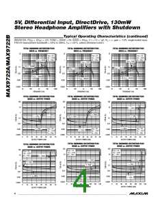
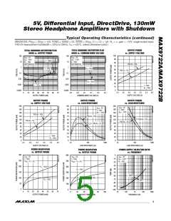
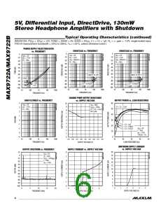
5V, Differential Input, DirectDrive, 130mW
Stereo Headphone Amplifiers with Shutdown
Detailed Description
The MAX9722A/MAX9722B stereo headphone amplifiers
feature Maxim’s DirectDrive architecture, eliminating the
large output-coupling capacitors required by conven-
V
V
DD
tional single-supply headphone amplifiers. The devices
consist of two class AB headphone amplifiers, undervolt-
age lockout (UVLO)/shutdown control, charge pump,
and comprehensive click-and-pop suppression circuitry
(see Typical Application Circuit). The charge pump
V
OUT
/2
DD
GND
inverts the positive supply (PV ), creating a negative
DD
supply (PV ). The headphone amplifiers operate from
SS
these bipolar supplies with their outputs biased about
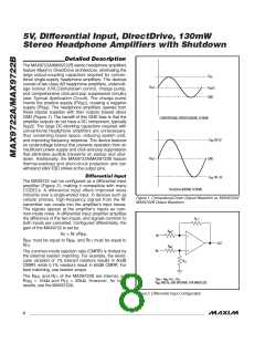
GND (Figure 1). The benefit of this GND bias is that the
amplifier outputs do not have a DC component, typically
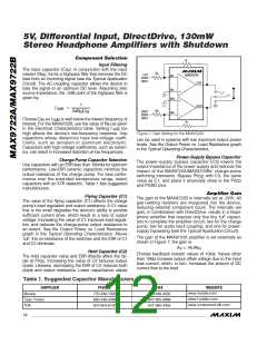
CONVENTIONAL DRIVER-BIASING SCHEME
V
/2. The large DC-blocking capacitors required with
DD
conventional headphone amplifiers are unnecessary,
thus conserving board space, reducing system cost,
and improving frequency response. The device features
an undervoltage lockout that prevents operation from an
insufficient power supply and click-and-pop suppression
that eliminates audible transients on startup and shut-
down. Additionally, the MAX9722A/MAX9722B feature
thermal-overload and short-circuit protection and can
withstand 8kV ESD strikes at the output pins.
+V OR 3V
DD
V
GND
OUT
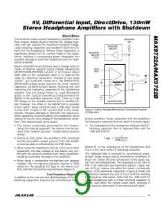
Differential Input
The MAX9722 can be configured as a differential input
amplifier (Figure 2), making it compatible with many
CODECs. A differential input offers improved noise
immunity over a single-ended input. In devices such as
cellular phones, high-frequency signals from the RF
transmitter can couple into the amplifier’s input traces.
The signals appear at the amplifier’s inputs as com-
mon-mode noise. A differential input amplifier amplifies
the difference of the two inputs, and signals common to
both inputs are cancelled. Configured differentially, the
gain of the MAX9722 is set by:
-V OR -3V
DD
DirectDrive BIASING SCHEME
Figure 1. Conventional Driver Output Waveform vs. MAX9722A/
MAX9722B Output Waveform
R
*
F1
R
IN1
*
A = R /R
V
F1 IN1
IN-
IN+
R
R
must be equal to R , and R must be equal to
IN2 F1
IN1
OUT
.
F2
R
IN2
The common-mode rejection ratio (CMRR) is limited by
the external resistor matching. For example, the worst-
case variation of 1% tolerant resistors results in 40dB
CMRR, while 0.1% resistors result in 60dB CMRR. For
best matching, use resistor arrays.
R
F2
The R
IN2
and R of the MAX9722B are internal, set
F1
IN1
R
= R , R = R
IN2 F1 F2
IN1
R
= 15kΩ and R
= 30kΩ. However, for best
F2
*R AND R ARE INTERNAL FOR MAX9722B.
IN1
F1
results, use the MAX9722A.
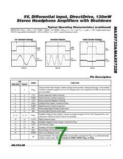
Figure 2. Differential Input Configuration
8
_______________________________________________________________________________________

 MAXIM [ MAXIM INTEGRATED PRODUCTS ]