5V, Differential Input, DirectDrive, 130mW
Stereo Headphone Amplifiers with Shutdown
Component Selection
R
F
Input Filtering
The input capacitor (C ), in conjunction with the input
IN
R
IN
resistor (R ), forms a highpass filter that removes the DC
IN
LEFT
AUDIO
INPUT
MAX9722A
INL-
bias from an incoming signal (see the Typical Application
Circuit). The AC-coupling capacitor allows the device to
bias the signal to an optimum DC level. Assuming zero
source impedance, the -3dB point of the highpass filter is
given by:
OUTL
INL+
INR+
1
OUTR
f
=
-3dB
R
IN
2πR C
RIGHT
AUDIO
INPUT
IN IN
INR-
Choose C so f
is well below the lowest frequency of
IN
-3dB
R
F
interest. For the MAX9722B, use the value of R as given
IN
in the Electrical Characteristics table. Setting f
too
-3dB
high affects the device’s low-frequency response. Use
capacitors whose dielectrics have low-voltage coeffi-
cients, such as tantalum or aluminum electrolytic.
Capacitors with high-voltage coefficients, such as ceram-
ics, can result in increased distortion at low frequencies.
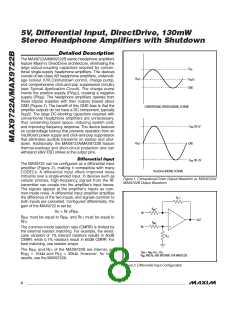
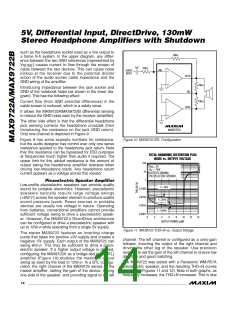
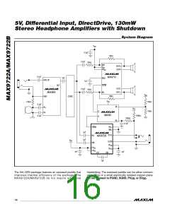
Figure 7. Gain Setting for the MAX9722A
can be used in systems with low maximum output power
levels. See the Output Power vs. Load Resistance graph
in the Typical Operating Characteristics.
Power-Supply Bypass Capacitor
The power-supply bypass capacitor (C3) lowers the
output impedance of the power supply and reduces the
impact of the MAX9722A/MAX9722Bs’ charge-pump
Charge-Pump Capacitor Selection
Use capacitors with an ESR less than 100mΩ for optimum
performance. Low-ESR ceramic capacitors minimize the
output resistance of the charge pump. For best perfor-
mance over the extended temperature range, select
capacitors with an X7R dielectric. Table 1 lists suggested
manufacturers.
switching transients. Bypass PV
with C3, the same
DD
value as C1, and place it physically close to the PV
and PGND pins.
DD
Amplifier Gain
The gain of the MAX9722B is internally set at -2V/V. All
gain-setting resistors are integrated into the device,
reducing external component count. The internally set
gain, in combination with DirectDrive, results in a head-
phone amplifier that requires only five tiny 1µF capaci-
tors to complete the amplifier circuit: two for the charge
pump, two for audio input coupling, and one for power-
supply bypassing (see the Typical Application Circuit).
Flying Capacitor (C1)
The value of the flying capacitor (C1) affects the charge
pump’s load regulation and output resistance. A C1 value
that is too small degrades the device’s ability to provide
sufficient current drive, which leads to a loss of output
voltage. Increasing the value of C1 improves load regula-
tion and reduces the charge-pump output resistance to
an extent. See the Output Power vs. Load Resistance
graph in the Typical Operating Characteristics. Above
1µF, the on-resistance of the switches and the ESR of C1
and C2 dominate.
The gain of the MAX9722A amplifier is set externally as
shown in Figure 7, the gain is:
A = -R /R
IN
V
F
Hold Capacitor (C2)
Choose feedback resistor values of 10kΩ. Values other
than 10kΩ increase output offset voltage due to the input
bias current, which, in turn, increases the amount of DC
current flow to the load.
The hold capacitor value and ESR directly affect the rip-
ple at PV . Increasing the value of C2 reduces output
SS
ripple. Likewise, decreasing the ESR of C2 reduces both
ripple and output resistance. Lower capacitance values
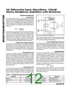
Table 1. Suggested Capacitor Manufacturers
SUPPLIER
PHONE
FAX
WEBSITE
www.murata.com
Murata
770-436-1300
800-348-2496
847-803-6100
770-436-3030
847-925-0899
847-390-4405
www.t-yuden.com
Taiyo Yuden
TDK
www.component.tdk.com
12 ______________________________________________________________________________________

 MAXIM [ MAXIM INTEGRATED PRODUCTS ]