5V, Differential Input, DirectDrive, 130mW
Stereo Headphone Amplifiers with Shutdown
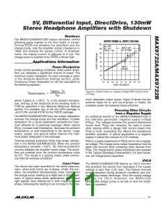
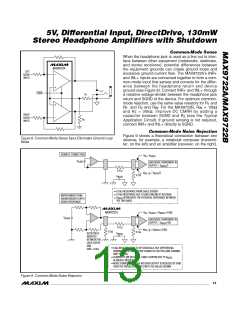
Common-Mode Sense
When the headphone jack is used as a line out to inter-
face between other equipment (notebooks, desktops,
and stereo receivers), potential differences between
MAX9722A
the equipment grounds can create ground loops and
LEFT
AUDIO
INPUT
excessive ground-current flow. The MAX9722A’s INR+
and INL+ inputs are connected together to form a com-
mon-mode input that senses and corrects for the differ-
ence between the headphone return and device
ground (see Figure 8). Connect INR+ and INL+ through
SHDN
R
1
a resistive voltage-divider between the headphone jack
return and SGND of the device. For optimum common-
mode rejection, use the same value resistors for R and
1
R , and R and R . For the MAX9722B, R = 15kΩ
F
2
IN
IN
and R = 30kΩ. Improve DC CMRR by adding a
F
RIGHT
AUDIO
INPUT
capacitor between SGND and R (see the Typical
2
R
2
Application Circuit). If ground sensing is not required,
connect INR+ and INL+ directly to SGND.
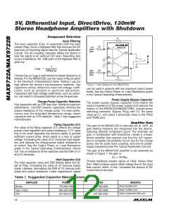
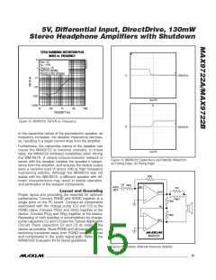
Common-Mode Noise Rejection
Figure 9 shows a theoretical connection between two
devices, for example, a notebook computer (transmit-
ter, on the left) and an amplifier (receiver, on the right),
Figure 8. Common-Mode Sense Input Eliminates Ground-Loop
Noise
EXAMPLE CONNECTION:
V
= V
AUDIO
IN
V
AUDIO
GND NOISE COMPONENT IN
OUTPUT = V /2
NOISE
0.1Ω
V
= V
/2
NOISE
REF_IN
0.1Ω
V
NOISE
0.10Ω RESISTANCE FROM CABLE SCREEN.
•
•
•
0.10Ω RESISTANCE DUE TO GND CABLING AT RECEIVER.
IMPROVEMENT FROM
ADDING MAX9722 WITH
SERIES RESISTANCE
V
REPRESENTS THE POTENTIAL DIFFERENCE BETWEEN
NOISE
THE TWO GNDS.
MAX9722A
V
= V
+ (V
x 0.98)
NOISE
IN
AUDIO
V
AUDIO
GND NOISE COMPONENT IN
OUTPUT = V /100
NOISE
0.1Ω
V
= (V
x 0.99)
NOISE
REF_IN
9.8Ω
0.1Ω
RESISTOR IS
INSERTED
V
NOISE
BETWEEN THE
JACK SLEEVE
AND
• 9.8Ω RESISTOR ADDS TO HP CROSSTALK, BUT DIFFERENTIAL
SENSING AT THE JACK SLEEVE CORRECTS FOR THIS (ONE CHANNEL
ONLY SHOWN).
GND = 9.8Ω
CURRENT FLOW (IN SIGNAL CABLE SCREEN) DUE TO V
IS GREATLY REDUCED.
•
NOISE
NOISE COMPONENT IN THE RECEIVER OUTPUT IS REDUCED BY 34dB
OVER THE PREVIOUS EXAMPLE WITH THE VALUES SHOWN.
•
Figure 9. Common-Mode Noise Rejection
______________________________________________________________________________________ 13

 MAXIM [ MAXIM INTEGRATED PRODUCTS ]