5V, Differential Input, DirectDrive, 130mW
Stereo Headphone Amplifiers with Shutdown
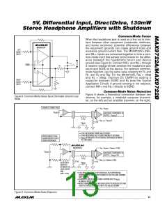
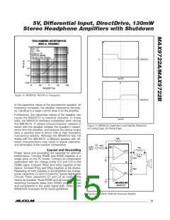
TOTAL HARMONIC DISTORTION PLUS
NOISE vs. FREQUENCY
10
V
DD
= 5V
A = -1V/V
V
V
= 2V
OUT(P-P)
1
0.1
OUTPUTS DRIVING
PIEZOELECTRIC SPEAKER
A
500mV/div
0.01
0.001
0.0001
4μs/div
10
100
1k
10k
100k
FREQUENCY (Hz)
Figure 12. MAX9722 THD+N vs. Frequency
B
500mV/div
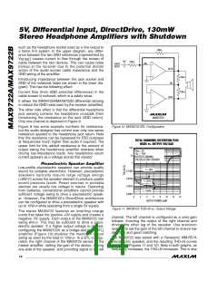
to the capacitive nature of the piezoelectric speaker, as
frequency increases, the speaker impedance decreas-
es, resulting in a larger current draw from the amplifier.
Furthermore, the capacitive nature of the speaker can
cause the MAX9722 to become unstable. In these
tests, the MAX9722 exhibited instabilities when driving
the WM-R57A. A simple inductor/resistor network in
series with the speaker isolates the speaker’s capaci-
tance from the amplifier, and ensures the device output
sees a resistive load of about 10Ω at high frequency
maintaining stability. Although the MAX9722 was not
stable with the WM-R57A, a different speaker with dif-
ferent characteristics may result in stable operation,
and elimination of the isolation components.
2μs/div
Figure 13. MAX9722 Capacitive-Load Stability Waveform:
(a) Falling Edge, (b) Rising Edge
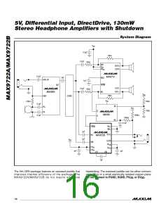
10kΩ
1μF
10kΩ
INR
AUDIO
INPUT
10Ω
Layout and Grounding
Proper layout and grounding are essential for optimum
performance. Connect PGND and SGND together at a
single point on the PC board. Connect all components
associated with the charge pump (C2 and C3) to the
OUTR
100μH
10kΩ
10kΩ
INL
PGND plane. Connect PV
and SV
SS
together at the
DD
DD
device. Connect PV and SV together at the device.
SS
Bypassing of both supplies is accomplished by charge-
pump capacitors C2 and C3 (see the Typical Application
Circuit). Place capacitors C2 and C3 as close to the
device as possible. Route PGND and all traces that carry
switching transients away from SGND and the traces
and components in the audio signal path. Refer to the
MAX9722A Evaluation Kit for layout guidelines.
OUTL
MAX9722A
Figure 14. Isolation Network Improves Stability
______________________________________________________________________________________ 15

 MAXIM [ MAXIM INTEGRATED PRODUCTS ]