SMBus Level 2 Battery Charger
with Remote Sense
The crossover frequency is given by:
the device). Unlike the DLO output, the DHI output uses
a 50ns (typ) delay time to prevent the low-side MOSFET
from turning on until DHI is fully off. The same consider-
ations should be used for routing the DHI signal to the
high-side MOSFET.
GMS
f
=
CO_CS
2πC
CS
For stability, choose a crossover frequency lower than
1/10 the switching frequency:
The high-side driver (DHI) swings from LX to 5V above
LX (BST) and has a typical impedance of 3Ω sourcing
and 1Ω sinking. The low-side driver (DLO) swings from
DLOV to ground and has a typical impedance of 1Ω
sinking and 3Ω sourcing. This helps prevent DLO from
being pulled up when the high-side switch turns on, due
to capacitive coupling from the drain to the gate of the
low-side MOSFET. This places some restrictions on the
MOSFETs that can be used. Using a low-side MOSFET
with smaller gate-to-drain capacitance can prevent
these problems.
C
= 5 × GMS/(2πf
)
CS
OSC
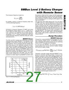
Choosing a crossover frequency of 30kHz and using
the component values listed in Figure 1 yields C
>
CS
5.4nF. Values for CCS greater than 10 times the mini-
mum value may slow down the current-loop response
excessively. Figure 12 shows the Bode plot of the input
current-limit-loop frequency response using the values
calculated above.
Design Procedure
MOSFET Selection
Choose the n-channel MOSFETs according to the maxi-
mum required charge current. The MOSFETs must be
able to dissipate the resistive losses plus the switching
MOSFET Drivers
The DHI and DLO outputs are optimized for driving
moderate-sized power MOSFETs. The MOSFET drive
capability is the same for both the low-side and high-
sides switches. This is consistent with the variable duty
factor that occurs in the notebook computer environ-
ment where the battery voltage changes over a wide
range. There must be a low-resistance, low-inductance
path from the DLO driver to the MOSFET gate to pre-
vent shoot-through. Otherwise, the sense circuitry in the
MAX8731A interprets the MOSFET gate as “off” while
there is still charge left on the gate. Use very short,
wide traces measuring 10 to 20 squares or less
(1.25mm to 2.5mm wide if the MOSFET is 25mm from
losses at both V
and V
.
DCIN(MAX)
DCIN(MIN)
For the high-side MOSFET, the worst-case resistive
power losses occur at the maximum battery voltage
and minimum supply voltage:
V
FBS_
2
PD
(HighSide) =
×I
×RDS(ON)
CONDUCTION
CHG
V
CSSP
Generally a low-gate charge high-side MOSFET is pre-
ferred to minimize switching losses. However, the
R
required to stay within package power-dissi-
DS(ON)
pation limits often limits how small the MOSFET can be.
The optimum occurs when the switching (AC) losses
100
80
60
40
20
0
0
MAG
PHASE
equal the conduction (R
) losses. Calculating the
DS(ON)
power dissipation in N1 due to switching losses is diffi-
cult since it must allow for difficult quantifying factors
that influence the turn-on and turn-off times. These fac-
tors include the internal gate resistance, gate charge,
threshold voltage, source inductance, and PCB layout
characteristics. The following switching-loss calculation
provides a rough estimate and is no substitute for
breadboard evaluation, preferably including a verifica-
tion using a thermocouple mounted on N1:
-45
-20
-40
-90
10M
1
2
0.1
10
1k
100k
PD
(High Side) = × t
× V ×I × f
DCIN CHG SW
SWITCHING
Trans
FREQUENCY (Hz)
Figure 12. CCS Loop Response
______________________________________________________________________________________ 27

 MAXIM [ MAXIM INTEGRATED PRODUCTS ]