SMBus Level 2 Battery Charger
with Remote Sense
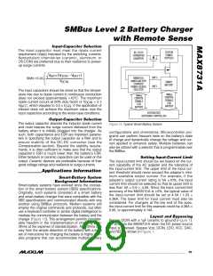
Good PCB layout is required to achieve specified noise
immunity, efficiency, and stable performance. The PCB
layout artist must be given explicit instructions—prefer-
ably, a sketch showing the placement of the power-
switching components and high-current routing. Refer to
the PCB layout in the MAX8731A evaluation kit for exam-
ples. A ground plane is essential for optimum perfor-
mance. In most applications, the circuit will be located
on a multilayer board, and full use of the four or more
copper layers is recommended. Use the top layer for
high-current connections, the bottom layer for quiet con-
nections, and the inner layers for uninterrupted ground
planes.
not go through vias. The resulting top-layer sub-
ground plane is connected to the normal inner-
layer ground plane at the paddle. Other
high-current paths should also be minimized, but
focusing primarily on short ground and current-
sense connections eliminates approximately 90%
of all PCB layout problems.
2) Place the IC and signal components. Keep the
main switching node (LX node) away from sensitive
analog components (current-sense traces and REF
capacitor).
Important: The IC must be no further than 10mm
from the current-sense resistors. Quiet connections
to REF, CCS, DAC, CCV, CCI, ACIN, and VCC
should be returned to a separate ground (GND)
island. The analog ground is separately worked
from power ground in Figure 1. There is very little
current flowing in these traces, so the ground island
need not be very large. When placed on an inner
layer, a sizable ground island can help simplify the
layout because the low-current connections can be
made through vias. The ground pad on the back-
side of the package should also be connected to
this quiet ground island.
Use the following step-by-step guide:
1) Place the high-power connections first, with their
grounds adjacent:
a) Minimize the current-sense resistor trace
lengths, and ensure accurate current sensing
with Kelvin connections.
b) Minimize ground trace lengths in the high-cur-
rent paths.
c) Minimize other trace lengths in the high-current
paths.
Use > 5mm wide traces in the high-current
paths.
3) Keep the gate-drive traces (DHI and DLO) as short
as possible (L < 20mm), and route them away from
the current-sense lines and REF. These traces
should also be relatively wide (W > 1.25mm).
d) Connect C1 and C2 to high-side MOSFET
(10mm max length). Place the input capacitor
between the input current-sense resistor and
drain of the high-side MOSFET.
4) Place ceramic bypass capacitors close to the IC.
The bulk capacitors can be placed further away.
Place the current-sense input filter capacitors under
the part, connected directly to the GND pin.
e) Minimize the LX node (MOSFETs, rectifier cath-
ode, inductor (15mm max length)). Keep LX on
one side of the PCB to reduce EMI radiation.
5) Use a single-point star ground placed directly
below the part at the PGND pin. Connect the power
ground (ground plane) and the quiet ground island
at this location.
f) Since the return path of DHI is LX, route DHI near
LX. Optimally, LX and DHI should overlap. The
same principle is applied to DLO and PGND.
g) Ideally, surface-mount power components are
flush against one another with their ground termi-
nals almost touching. These high-current
grounds are then connected to each other with a
wide, filled zone of top-layer copper, so they do
Chip Information
TRANSISTOR COUNT: 10,234
PROCESS: BiCMOS
30 ______________________________________________________________________________________

 MAXIM [ MAXIM INTEGRATED PRODUCTS ]