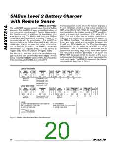
SMBus Level 2 Battery Charger
with Remote Sense
greater than 10MΩ. The voltage amplifier transconduc-
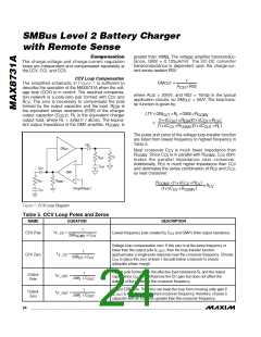
Compensation
The charge-voltage and charge-current regulation
loops are independent and compensated separately at
the CCV, CCI, and CCS.
tance, GMV = 0.125µA/mV. The DC-DC converter
transconductance is dependent upon the charge-cur-
rent sense resistor RS2:
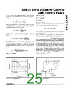
CCV Loop Compensation
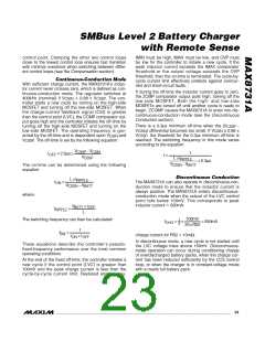
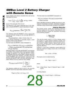
The simplified schematic in Figure 7 is sufficient to
describe the operation of the MAX8731A when the volt-
age loop (CCV) is in control. The required compensa-
1
GM
=
OUT
A
×RS2
CSI
where A
= 20V/V, and RS2 = 10mΩ in the typical
CSI
tion network is a pole-zero pair formed with C
and
CV
application circuits, so GM
fer function is given by:
= 5A/V. The loop-trans-
OUT
R
. The zero is necessary to compensate the pole
formed by the output capacitor and the load. R
CV
is
ESR
the equivalent series resistance (ESR) of the charger
output capacitor (C ). R is the equivalent charger
LTF = GM
×R ×GMV ×R
L OGMV
OUT
OUT
L
output load, where R = ΔV
/ ΔI . The equiva-
(1+sC
×R
)(1+sC ×R
)
L
BATT
CHG
OUT
ESR
CV
CV
×
lent output impedance of the GMV amplifier, R
, is
OGMV
(1+sC ×R
)(1+sC
×R )
CV
OGMV
OUT L
The poles and zeros of the voltage loop-transfer function
are listed from lowest frequency to highest frequency in
Table 5.
FBS_
GM
OUT
Near crossover C
is much lower impedance than
CV
R
. Since C is in parallel with R
, C dom-
OGMV
CV
OGMV CV
R
L
R
ESR
inates the parallel impedance near crossover.
Additionally, R
is much higher impedance than C
CV
CV
C
OUT
CCV
and dominates the series combination of R and C
,
CV
CV
GMV
so near crossover:
R
CV
R
OGMV
R
× (1+sC ×R
)
OGMV
CV
CV
≅R
CV
ChargeVoltage( )
(1+sC ×R
)
CV
OGMV
C
CV
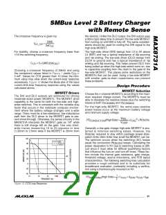
Figure 7. CCV Loop Diagram
Table 5. CCV Loop Poles and Zeros
NAME
EQUATION
DESCRIPTION
1
f
=
CCV Pole
Lowest frequency pole created by C and GMV’s finite output resistance.
CV
P_CV
2πR
× C
CV
OGMV
Voltage-loop compensation zero. If this zero is at the same frequency or
lower than the output pole f
, then the loop-transfer function
P_OUT
1
f
=
CCV Zero
approximates a single-pole response near the crossover frequency. Choose
to place this zero at least 1 decade below crossover to ensure
Z_CV
2πR × C
CV
CV
C
CV
adequate phase margin.
Output pole formed with the effective load resistance R and the output
L
1
Output
Pole
f
f
=
=
P_OUT
P_OUT
capacitance C . R influences the DC gain but does not affect the
OUT L
2πR × C
L
OUT
OUT
stability of the system or the crossover frequency.
Output ESR Zero. This zero can keep the loop from crossing unity gain if
1
Output
Zero
f
is less than the desired crossover frequency; therefore, choose a
Z_OUT
2πR × C
L
capacitor with an ESR zero greater than the crossover frequency.
24 ______________________________________________________________________________________

 MAXIM [ MAXIM INTEGRATED PRODUCTS ]