SMBus Level 2 Battery Charger
with Remote Sense
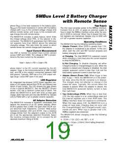
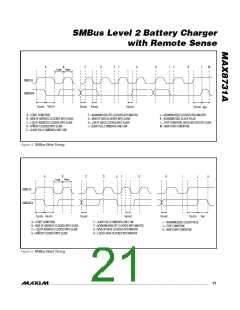
Communication starts when the master signals a
SMBus Interface
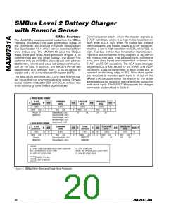
The MAX8731A receives control inputs from the SMBus
interface. The MAX8731A uses a simplified subset of
the commands documented in System Management
Bus Specification V1.1, which can be downloaded from
www.smbus.org. The MAX8731A uses the SMBus
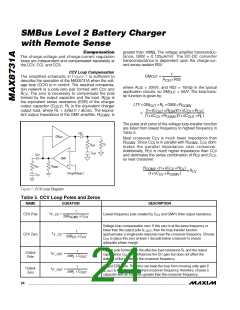
Read-Word and Write-Word protocols (Figure 3) to
communicate with the smart battery. The MAX8731A
performs only as an SMBus slave device with address
0b0001001_ (0x12) and does not initiate communica-
tion on the bus. In addition, the MAX8731A has two
identification (ID) registers (0xFE): a 16-bit device ID
register and a 16-bit manufacturer ID register (0xFF).
START condition, which is a high-to-low transition on
SDA, while SCL is high. When the master has finished
communicating, the master issues a STOP condition,
which is a low-to-high transition on SDA, while SCL is
high. The bus is then free for another transmission.
Figures 4 and 5 show the timing diagram for signals on
the SMBus interface. The address byte, command
byte, and data bytes are transmitted between the
START and STOP conditions. The SDA state changes
only while SCL is low, except for the START and STOP
conditions. Data is transmitted in 8-bit bytes and is
sampled on the rising edge of SCL. Nine clock cycles
are required to transfer each byte in or out of the
MAX8731A because either the master or the slave
acknowledges the receipt of the correct byte during the
ninth clock cycle. The MAX8731A supports the charger
commands as described in Table 4.
The data (SDA) and clock (SCL) pins have Schmitt-trig-
ger inputs that can accommodate slow edges. Choose
pullup resistors (10kΩ) for SDA and SCL to achieve rise
times according to the SMBus specifications.
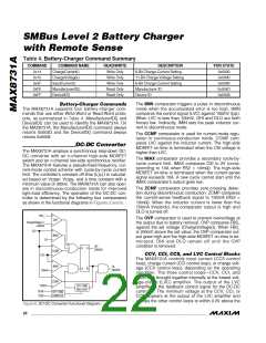
a) WRITE-WORD FORMAT
SLAVE
ADDRESS
COMMAND
BYTE
LOW DATA
BYTE
HIGH DATA
BYTE
S
W
ACK
ACK
ACK
ACK
P
7 BITS
1b 1b
8 BITS
1b
0
8 BITS
1b
0
8 BITS
1b
0
MSB
LSB
0
0
MSB
LSB
MSB
D7
LSB
D0
MSB
LSB
D8
PRESET TO
0b0001001
ChargerMode() = 0x12
ChargeCurrent() = 0x14
ChargeVoltage() = 0x15
AlarmWarning() = 0x16
InputCurrent() = 0x3F
D15
b) READ-WORD FORMAT
SLAVE
COMMAND
BYTE
SLAVE
ADDRESS
LOW DATA
BYTE
HIGH DATA
BYTE
S
W
ACK
ACK
S
R
ACK
ACK
NACK P
ADDRESS
7 BITS
1b 1b
8 BITS
1b
0
7 BITS
1b 1b
8 BITS
1b
0
8 BITS
1b
1
MSB
Preset to
0b0001001
LSB
0
0
MSB
LSB
MSB
LSB
1
0
MSB
D7
LSB
D0
MSB
D15
LSB
D8
ChargerSpecInfo() = 0x11
ChargerStatus() = 0x13
PRESET TO
0b0001001
LEGEND:
S = START CONDITION OR REPEATED START CONDITION
ACK = ACKNOWLEDGE (LOGIC-LOW)
W = WRITE BIT (LOGIC-LOW)
P = STOP CONDITION
NACK = NOT ACKNOWLEDGE (LOGIC-HIGH)
R = READ BIT (LOGIC-HIGH)
MASTER TO SLAVE
SLAVE TO MASTER
Figure 3. SMBus Write-Word and Read-Word Protocols
20 ______________________________________________________________________________________

 MAXIM [ MAXIM INTEGRATED PRODUCTS ]