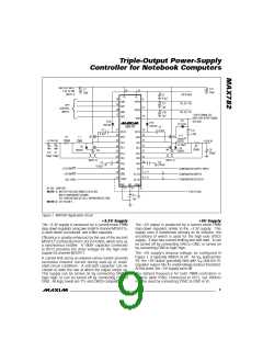
Trip le -Ou t p u t P o w e r-S u p p ly
Co n t ro lle r fo r No t e b o o k Co m p u t e rs
forward mode. The low impedance presented by the
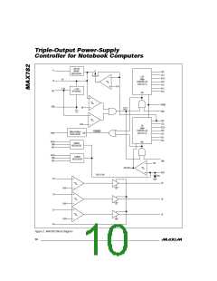
+3 .3 V a n d +5 V P WM Bu c k Co n t ro lle rs
The two current-mode PWM controllers are identical
except for different preset output voltages and the
addition of a flyback winding control loop to the +5V
side (see Figure 3, +3.3V/+5V PWM Controller Block
Diagram). Each PWM is independent except for being
synchronized to a master oscillator and sharing a com-
mon reference (REF) and logic supply (VL). Each PWM
can be turned on and off separately via ON3 and ON5.
The PWMs are a direct-summing type, lacking a tradi-
tional integrator-type error amplifier and the phase shift
associated with it. They therefore do not require any
external feedback compensation components if the fil-
te r c a p a c itor ESR g uid e line s g ive n in the De s ig n
Procedure are followed.
tra ns forme r s e c ond a ry in forwa rd mod e a llows the
+15V filte r c a p a c itor to b e q uic kly c ha rg e d a g a in,
bringing VDD into regulation.
Soft-Start/SS_ Inputs
Connecting capacitors to SS3 and SS5 allows gradual
build-up of the +3.3V and +5V supplies after ON3 and
ON5 are driven high. When ON3 or ON5 is low, the
appropriate SS capacitors are discharged to GND.
When ON3 or ON5 is driven high, a 4µA constant cur-
rent source charges these capacitors up to 4V. The
resulting ramp voltage on the SS_ pins linearly increas-
e s the c urre nt-limit c omp a ra tor s e tp oint s o a s to
increase the duty cycle to the external power MOSFETs
up to the maximum output. With no SS capacitors, the
circuit will reach maximum current limit within 10µs.
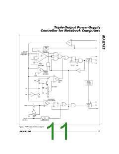
MAX782
The main gain block is an open-loop comparator that
sums four input signals: an output voltage error signal,
current-sense signal, slope-compensation ramp, and
p re c is ion volta g e re fe re nc e . This d ire c t-s umming
method approaches the ideal of cycle-by-cycle control
of the output voltage. Under heavy loads, the controller
operates in full PWM mode. Every pulse from the oscil-
lator sets the output latch and turns on the high-side
s witc h for a p e riod d e te rmine d b y the d uty c yc le
Soft-start greatly reduces initial in-rush current peaks
and allows start-up time to be programmed externally.
Synchronous Rectifiers
Synchronous rectification allows for high efficiency by
reducing the losses associated with the Schottky recti-
fiers. Also, the synchronous rectifier MOSFETS are
necessary for correct operation of the MAX782's boost
gate-drive and VDD supplies.
(approximately V /V ). As the high-side switch turns
OUT IN
off, the synchronous rectifier latch is set and, 60ns later,
the low-side switch turns on (and stays on until the
beginning of the next clock cycle, in continuous mode,
or until the inductor current crosses through zero, in
discontinuous mode). Under fault conditions where the
ind uc tor c urre nt e xc e e d s the 100mV c urre nt-limit
threshold, the high-side latch is reset and the high-side
switch is turned off.
When the external power MOSFET N1 (or N2) turns off,
energy stored in the inductor causes its terminal volt-
age to reverse instantly. Current flows in the loop
formed by the inductor, Schottky diode, and load, an
action that charges up the filter capacitor. The Schottky
d iod e ha s a forwa rd volta g e of a b out 0.5V whic h,
although small, represents a significant power loss,
degrading efficiency. A synchronous rectifier, N3 (or
N4), parallels the diode and is turned on by DL3 (or
DL5) shortly after the diode conducts. Since the on
At light loads, the inductor current fails to exceed the
25mV threshold set by the minimum current compara-
tor. When this occurs, the PWM goes into idle-mode,
skipping most of the oscillator pulses in order to reduce
the switching frequency and cut back switching losses.
The osc illa tor is e ffe c tive ly ga te d off a t lig ht loa ds
because the minimum current comparator immediately
resets the high-side latch at the beginning of each
cycle, unless the FB_ signal falls below the reference
voltage level.
resistance (r ) of the synchronous rectifier is very
DS(ON)
low, the losses are reduced.
The synchronous rectifier MOSFET is turned off when
the inductor current falls to zero.
Cross conduction (or “shoot-through”) is said to occur
if the high-side switch turns on at the same time as the
synchronous rectifier. The MAX782’s internal break-
before-make timing ensures that shoot-through does not
occur. The Schottky rectifier conducts during the time
that neither MOSFET is on, which improves efficiency
b y p re ve nting the s ync hronous -re c tifie r MOSFET’s
lossy body diode from conducting.
A flyback winding controller regulates the +15V VDD
supply in the absence of a load on the main +5V out-
put. If VDD falls below the preset +13V VDD regulation
threshold, a 1µs one-shot is triggered that extends the
on-time of the low-side switch beyond the point where
the inductor current crosses zero (in discontinuous
mod e ). This c a us e s ind uc tor (p rima ry) c urre nt to
reverse, pulling current out of the output filter capacitor
and causing the flyback transformer to operate in the
The synchronous rectifier works under all operating condi-
tions, including discontinuous-conduction and idle-mode.
The +5V synchronous rectifier also controls the 15V VDD
voltage (see the High-Side Supply (VDD) section).
12 ______________________________________________________________________________________

 MAXIM [ MAXIM INTEGRATED PRODUCTS ]