+5V, Serial-Input, Voltage-Output, 14-Bit DACs
Pin Descriptions (continued)
MAX545
PIN
1
NAME
RFS
FUNCTION
Feedback Resistor. Connect to external op amp’s output in bipolar mode.
DAC Output Voltage
ꢂ
OUT
3
AGIDF
AGIDL
REFL
REFF
CS
Analog Ground (force)
4
Analog Ground (sense)
5
Voltage Reference ꢁnput (sense). Connect REFL to external +ꢂ.5V reference.
Voltage Reference ꢁnput (force). Connect REFF to external +ꢂ.5V reference.
Chip-Lelect ꢁnput
6
7
8
LCꢀK
I.C.
Lerial-Clock ꢁnput. Duty cycle must be between 4±% and 6±%.
Io Connection. Iot internally connected.
Lerial-Data ꢁnput
0
1±
11
1ꢂ
DꢁI
LDAC
DGID
LDAC ꢁnput. A falling edge updates the internal DAC latch.
Digital Ground
Junction of internal scaling resistors. Connect to external op amp’s inverting input in
bipolar mode.
13
14
ꢁIV
V
DD
+5V Lupply Voltage
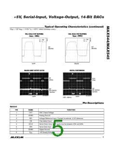
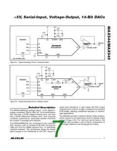
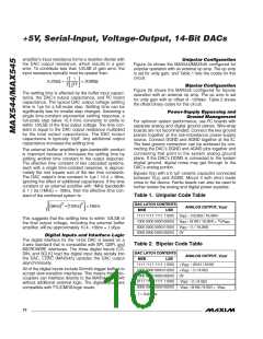
t
t
CSH1
LDACS
CS
t
CSHO
t
CSS1
t
t
t
CL
CSSO
CH
SCLK
t
DH
t
DS
D13
D12
S0
DIN
LDAC*
t
LDAC
*MAX545 ONLY
Figure 1. Timing Diagram
6
_______________________________________________________________________________________

 MAXIM [ MAXIM INTEGRATED PRODUCTS ]