+5V, Serial-Input, Voltage-Output, 14-Bit DACs
Digital Interface
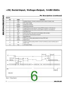
The MAX544/MAX545’s digital interface is a standard
3-wire connection compatible with LPꢁ/QLPꢁ/
MꢁCROWꢁRE interfaces. The chip-select input (CS)
frames the serial data loading at the data-input pin
(DꢁI). ꢁmmediately following CS’s high-to-low transition,
the data is shifted synchronously and latched into the
input register on the rising edge of the serial clock input
(LCꢀK). After 16 bits (14 data bits, plus ꢂ sub-bits set to
zero) have been loaded into the serial input register, it
transfers its contents to the DAC latch on CS’s low-to-
high transition (Figure 3a). Iote that if CS is not kept
low during the entire 16 LCꢀK cycles, data will be cor-
rupted. ꢁn this case, reload the DAC latch with a new
16-bit word.
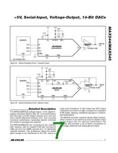
External Reference
The MAX544/MAX545 operate with external voltage ref-
erences from ꢂV to 3V. The reference voltage deter-
mines the DAC’s full-scale output voltage. Kelvin
connections are provided with the MAX545 for optimum
performance. The ꢂ.5V MAX873A, with ±15mV initial
accuracy and a 7ppm/°C (max) temperature coeffi-
cient, is a good choice.
Power-On Reset
The MAX544/MAX545 have a power-on reset circuit to
set the DAC’s output to ±V in unipolar mode when V
DD
is first applied. This ensures that unwanted DAC output
voltages will not occur immediately following a system
power-up, such as after a loss of power. ꢁn bipolar
mode, the DAC output is set to -V
.
REF
Alternatively, for the MAX545, LDAC allows the DAC
latch to update asynchronously by pulling LDAC low
after CS goes high (Figure 3b). Hold LDAC high during
the data-loading sequence.
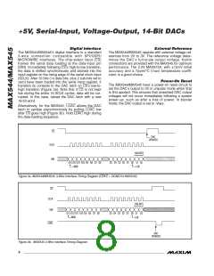
CS
DAC
UPDATED
SCLK
SUB-BITS
DIN
D13 D12 D11 D10 D9 D8 D7 D6
MSB
D5 D4 D3 D2 D1 D0 S1 S0
LSB
Figure 3a. MAX544/MAX545 3-Wire Interface Timing Diagram (LDAC = DGND for MAX545)
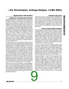
CS
SCLK
SUB-BITS
DIN
D13 D12 D11 D10 D9 D8 D7 D6
MSB
D5 D4 D3 D2 D1 D0 S1 S0
LSB
LDAC
DAC
UPDATED
Figure 3b. MAX545 4-Wire Interface Timing Diagram
8
_______________________________________________________________________________________

 MAXIM [ MAXIM INTEGRATED PRODUCTS ]